Manufacturing method for uncovering multiple layers in same area of multilayer circuit board

A technology of multi-layer circuit and production method, which is applied in multi-layer circuit manufacturing, printed circuit manufacturing, removing conductive materials by chemical/electrolytic methods, etc., can solve the problems of different laser depths, missing laser parameters, difficult to control and other problems , to achieve the effect of being conducive to lamination, avoiding different laser depths, and easy to control process parameters

Pending Publication Date: 2022-07-29
MFLEX YANCHENG CO LTD
View PDF0 Cites 0 Cited by
  • Summary
  • Abstract
  • Description
  • Claims
  • Application Information

AI Technical Summary

Problems solved by technology

[0011] In view of this, the present invention provides a multi-layer manufacturing method of opening the cover in the same area of ​​the multi-layer circuit board, so as to solve the problem of poor lamination and step-by-step front opening caused by a single step with a high d

Method used


Image

  • Manufacturing method for uncovering multiple layers in same area of multilayer circuit board
  • Manufacturing method for uncovering multiple layers in same area of multilayer circuit board
  • Manufacturing method for uncovering multiple layers in same area of multilayer circuit board

Examples


Example Embodiment

[0072] In order to make the purposes, technical solutions and advantages of the embodiments of the present invention clearer, the technical solutions in the embodiments of the present invention will be clearly and completely described below with reference to the accompanying drawings in the embodiments of the present invention. Obviously, the described embodiments These are some embodiments of the present invention, but not all embodiments. Based on the embodiments of the present invention, all other embodiments obtained by those skilled in the art without creative efforts shall fall within the protection scope of the present invention.

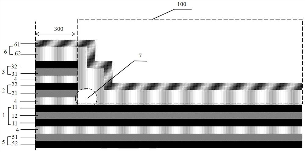
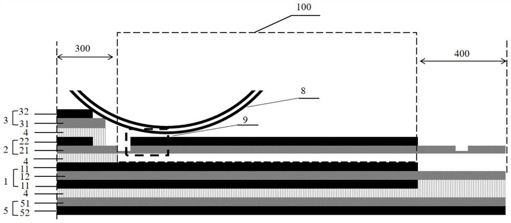
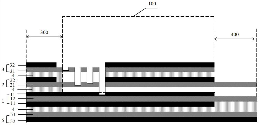
[0073] The embodiment of the present invention provides a method for manufacturing multiple layers by opening the cover in the same area of ​​a multilayer circuit board, such as Figure 4 shown, including the following steps:

[0074] S1: Press a first single-sided copper-clad substrate on one side of the double-sided copper-clad substrate t...


PUM


Abstract

The invention discloses a manufacturing method for uncovering multiple layers in the same area of a multilayer circuit board, which comprises the following steps of: pressing a first single-sided copper-clad substrate on one side of a double-sided copper-clad substrate to form a first multilayer board; pre-etching the first multilayer board according to a preset uncovering area; punching the second single-sided copper-clad substrate according to a preset uncovering area to form a receding groove penetrating through the second single-sided copper-clad substrate; according to a preset uncovering area, laminating and etching the punched second single-sided copper-clad substrate and the pre-etched first multi-layer board in sequence to obtain a second multi-layer board; and judging whether the second multilayer board meets a preset uncovering layer number or not, and sequentially performing laser and adhesive tearing on the second multilayer board according to a preset uncovering area and a judgment result to obtain a target multilayer board of which multiple layers are uncovered in the same area. According to the invention, the problems of poor lamination caused by a single high-fall step and missing tearing caused by the height difference of the board surface are avoided, and the yield of uncovering multiple layers in the same area of the multilayer board is improved.

Description

technical field [0001] The invention relates to the technical field of manufacture of flexible circuit boards, in particular to a manufacture method of opening a cover and multiple layers in the same area of ​​a multilayer circuit board. Background technique [0002] Flexible Printed Circuit (FPC or Flex for short) is a highly reliable and excellent flexible printed circuit board made of polyimide (PI) or polyester film as the base material. . Flexible circuit boards are divided into single-sided, double-sided and multi-layer boards (three or more layers) according to thickness and number of layers. Because the higher the number of layers and the thicker the thickness of the flexible circuit board, the worse the bending performance and the reliability cannot meet the requirements. Therefore, in the design of conventional flexible circuit boards, single-sided and double-sided manufacturing processes are used for circuit boards that need to be bent. [0003] However, as ele...

Claims


Application Information

Patent Timeline
IPC IPC(8): H05K3/46H05K3/06H05K3/00
CPCH05K3/4644H05K3/06H05K3/0044H05K3/4652
Inventor 吉一林唐晓锋杨锋
Owner MFLEX YANCHENG CO LTD
Why Eureka
Try Eureka