Epitaxial structure of light emitting diode and preparation method thereof

A technology of light-emitting diodes and epitaxial structures, applied in semiconductor devices, electrical components, circuits, etc., can solve the problems of reduced light-emitting diode luminous efficiency, high defect density and polarization effect, large lattice mismatch and thermal mismatch, etc. Achieve the effect of improving electron-hole recombination efficiency, preventing non-radiative recombination, and reducing the difference in electron-hole concentration

Pending Publication Date: 2022-08-02
XIAMEN SILAN ADVANCED COMPOUND SEMICON CO LTD +1
View PDF0 Cites 5 Cited by
  • Summary
  • Abstract
  • Description
  • Claims
  • Application Information

AI Technical Summary

Problems solved by technology

[0003] Light-emitting diodes usually use nitride semiconductor epitaxial layers. Traditional nitride semiconductor epitaxial layers usually use heterogeneous substrates. The lattice mismatch and thermal mismatch between the heterogeneous substrates and nitride epitaxial layers are relatively large, resulting in relatively large High defect density and polarization effects, resulting in non-radiative recombination and spatial separation of electronic wave functions, reduce the luminous efficiency of LEDs

Method used


Image

  • Epitaxial structure of light emitting diode and preparation method thereof
  • Epitaxial structure of light emitting diode and preparation method thereof
  • Epitaxial structure of light emitting diode and preparation method thereof

Examples


Embodiment Construction

[0045] The present invention will be described in more detail below with reference to the accompanying drawings. In the various figures, identical components are designated by similar reference numerals. For the sake of clarity, various parts in the figures have not been drawn to scale. Additionally, some well-known parts may not be shown.

[0046] The invention may be embodied in various forms, some examples of which will be described below.

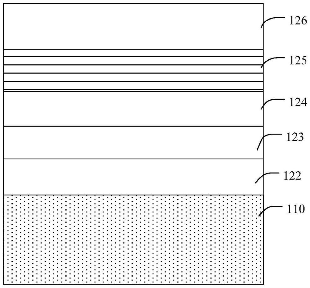
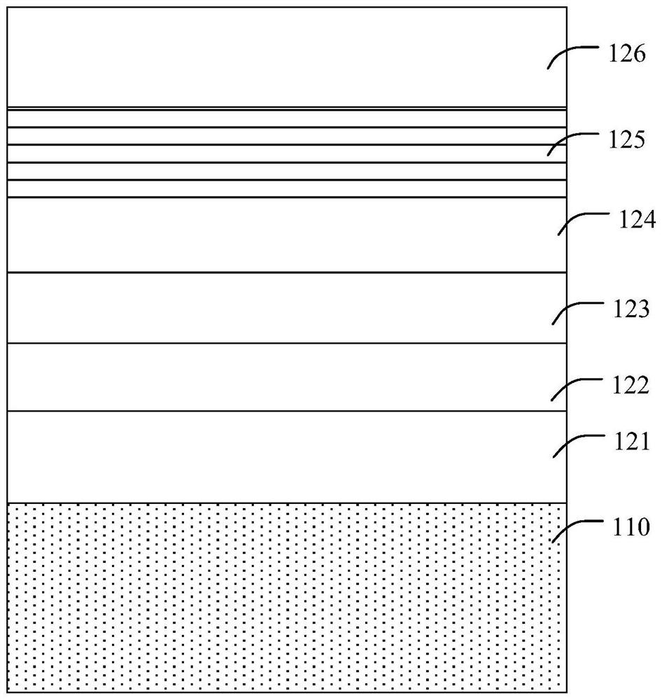
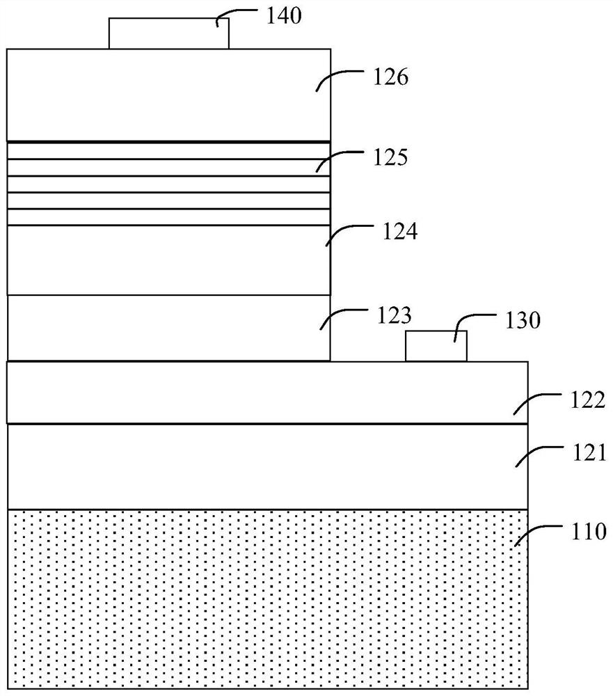
[0047] In the prior art, due to the lattice mismatch and thermal mismatch between the substrate and the epitaxial layer, the epitaxial layer produces a higher defect density and polarization reaction, thereby producing non-radiative recombination and spatial separation of the electron wave function, and further. Reduce the luminous efficiency of light-emitting diodes. Specifically, since the hole ionization efficiency of the epitaxial layer is much lower than the electron ionization efficiency, the hole concentration is 1 to 2 orders...


PUM


Abstract

The invention discloses an epitaxial structure of a light-emitting diode and a preparation method thereof. The epitaxial structure of the light-emitting diode comprises a substrate; the first semiconductor layer, the first barrier layer, the second barrier layer, the multi-quantum well layer and the second semiconductor layer are sequentially stacked on the substrate, doping types of the first barrier layer and the second semiconductor layer are opposite to each other, and the first semiconductor layer, the first barrier layer, the second barrier layer, the multi-quantum well layer and the second semiconductor layer are respectively subjected to carbon doping. And the carbon doping concentration of the multi-quantum well layer is less than or equal to the carbon doping concentration of the first barrier layer and less than or equal to the carbon doping concentration of the first semiconductor layer and less than or equal to the carbon doping concentration of the second barrier layer and less than or equal to the carbon doping concentration of the second semiconductor layer. According to the epitaxial structure of the light-emitting diode and the preparation method of the epitaxial structure, through setting the change of the carbon doping concentration of each layer in the epitaxial structure, the speed of injecting electrons into a multi-quantum well is reduced, and the probability that the electrons overflow from the multi-quantum well is reduced, so that the light-emitting efficiency of the light-emitting diode is improved.

Description

technical field [0001] The invention relates to the technical field of semiconductors, in particular to an epitaxial structure of a light emitting diode and a preparation method thereof. Background technique [0002] Light-emitting diodes (LEDs) have the characteristics of energy saving and environmental protection, high luminous efficiency, low cost, long life, wide wavelength range (such as 200nm ~ 1100nm), and small size. Therefore, in the field of traditional lighting, light-emitting diodes have completely replaced incandescent and fluorescent lamps. , become the light source of ordinary household lighting. And light-emitting diodes can also be used in Mini-LED, indoor high-resolution display, outdoor display, mobile phone backlight, TV backlight, notebook computer backlight, household lamps, street lamps, car lights, flashlights and other fields. [0003] Light-emitting diodes usually use nitride semiconductor epitaxial layers, and traditional nitride semiconductor epi...

Claims


Application Information

Patent Timeline
Patent Type & Authority Applications(China)
IPC IPC(8): H01L33/30H01L33/32H01L33/14H01L33/06H01L33/00
CPCH01L33/305H01L33/32H01L33/14H01L33/06H01L33/0075
Inventor 郑锦坚王曼常亮高默然毕京锋
Owner XIAMEN SILAN ADVANCED COMPOUND SEMICON CO LTD
Why Eureka
Try Eureka