Semiconductor light-emitting device and preparation method and test method thereof

A technology of light-emitting devices and semiconductors, applied to semiconductor lasers, structural details of semiconductor lasers, laser components, etc., can solve problems such as resource waste, cycle thickness deviation, and process cost increase, so as to reduce process costs and resources wasteful effect

Active Publication Date: 2022-08-09
SUZHOU EVERBRIGHT PHOTONICS CO LTD +1
View PDF4 Cites 0 Cited by
  • Summary
  • Abstract
  • Description
  • Claims
  • Application Information

AI Technical Summary

Problems solved by technology

[0003] Therefore, the technical problem to be solved by the present invention is to solve the difficulty in judging whether the periodic thickness of the first Bragg reflector or the periodic thickness of the second Bragg reflector deviates from the diffractio

Method used


Image

  • Semiconductor light-emitting device and preparation method and test method thereof
  • Semiconductor light-emitting device and preparation method and test method thereof
  • Semiconductor light-emitting device and preparation method and test method thereof

Examples


Embodiment 1

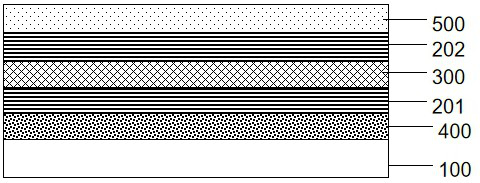
[0036] This embodiment provides a semiconductor light-emitting device, with reference to figure 1 and figure 2 ,include:

[0037] semiconductor substrate layer 100;

[0038] a first Bragg mirror 201 on the semiconductor substrate layer 100;

[0039] an active layer 300 located on the first Bragg mirror away from the semiconductor substrate layer;

[0040] a second Bragg mirror 202 located in the active layer 300 away from the first Bragg mirror 201;

[0041] Both the first Bragg mirror 201 and the second Bragg mirror 202 have bulk atom groups; the first Bragg mirror 201 or the second Bragg mirror 202 has lattice adjustment atoms, and the The diffraction angle corresponding to the diffraction peak of the first Bragg mirror 201 is different from the diffraction angle corresponding to the diffraction peak of the second Bragg mirror 202 , and the lattice adjustment atoms are different from atoms in the bulk atomic group.

[0042] In the semiconductor light emitting device pr...

Embodiment 2

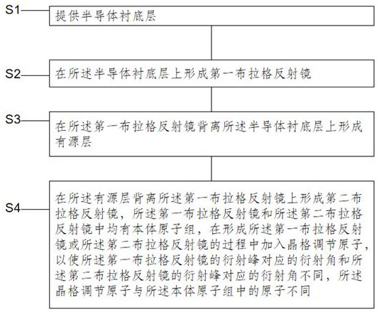
[0064] This embodiment provides a preparation method of a semiconductor light-emitting device, refer to image 3 , including the following steps:

[0065] Step S1: providing a semiconductor substrate layer;

[0066] Step S2: forming a first Bragg mirror on the semiconductor substrate layer;

[0067] Step S3: forming an active layer on the first Bragg mirror facing away from the semiconductor substrate layer;

[0068] Step S4: forming a second Bragg reflector on the active layer away from the first Bragg reflector, the first Bragg reflector and the second Bragg reflector both have bulk atomic groups, and after forming the second Bragg reflector. In the process of the first Bragg mirror or the second Bragg mirror, lattice adjustment atoms are added, so that the diffraction peak of the first Bragg mirror corresponds to the diffraction angle and the diffraction peak of the second Bragg mirror The corresponding diffraction angles are different, and the lattice adjustment atoms a...

Embodiment 3

[0100] This embodiment provides a method for testing a semiconductor light-emitting device, including:

[0101] The semiconductor light-emitting device described in Embodiment 1;

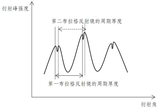
[0102] acquiring diffraction spectra of the first Bragg mirror and the second Bragg mirror;

[0103] Obtain the periodic thickness of the first Bragg mirror according to the diffraction angle corresponding to the diffraction peak of the first Bragg mirror in the diffraction spectrum;

[0104] The periodic thickness of the second Bragg mirror is obtained according to the diffraction angle corresponding to the diffraction peak of the second Bragg mirror in the diffraction spectrum.

[0105] In one embodiment, by comparing the periodic thickness of the first Bragg mirror and the periodic thickness of the second Bragg mirror, it is determined whether there is a deviation in the periodic thickness of the first Bragg mirror and the second Bragg mirror, On the basis of the deviation of the periodic thick...


PUM

PropertyMeasurementUnit
Thicknessaaaaaaaaaa
Thicknessaaaaaaaaaa
Thicknessaaaaaaaaaa

Abstract

The invention relates to a semiconductor light-emitting device and a preparation method and a test method thereof, and the semiconductor light-emitting device comprises a semiconductor substrate layer; a first Bragg reflector; an active layer; a second Bragg reflector; body atom groups are arranged in the first Bragg reflector and the second Bragg reflector; the first Bragg reflector or the second Bragg reflector is provided with lattice adjusting atoms, a diffraction angle corresponding to a diffraction peak of the first Bragg reflector is different from a diffraction angle corresponding to a diffraction peak of the second Bragg reflector, and the lattice adjusting atoms are different from atoms in the body atom group. The semiconductor device can judge whether the periodic thickness of the first Bragg reflector deviates or the periodic thickness of the second Bragg reflector deviates through the diffraction spectrum, so that the process cost is reduced, and the resource waste is reduced.

Description

technical field [0001] The present invention relates to the technical field of semiconductors, in particular to a semiconductor light-emitting device and a preparation method and testing method thereof. Background technique [0002] Due to the advantages of good beam quality, low threshold current, easy two-dimensional array integration, low manufacturing cost and mass production, semiconductor light-emitting devices have become a series of high optical power such as 3D sensing, lidar, night vision lighting, health care, etc. important light source for the application. The semiconductor light-emitting device includes three parts: a first Bragg mirror, a second Bragg mirror and an intermediate active layer. The influence of the periodic thickness of the first Bragg mirror and the periodic thickness of the second Bragg mirror on the wavelength of the semiconductor light-emitting device is very critical. Therefore, before growing the overall structure of the semiconductor ligh...

Claims


Application Information

Patent Timeline
IPC IPC(8): H01S5/183H01S5/02G01M11/02
CPCH01S5/18361H01S5/0206G01M11/02
Inventor 夏明月肖垚王俊郭银涛方砚涵肖啸程洋杨火木邓国亮周昊张弘
Owner SUZHOU EVERBRIGHT PHOTONICS CO LTD
Why Eureka
Try Eureka