Integral microchip laser with frequency modulation function

A microchip laser and frequency modulation technology, applied in lasers, laser parts, phonon exciters, etc., can solve the problems of stable and reliable operation of device manufacturing, and achieve the effects of improving stability, reducing costs, and compacting devices

Inactive Publication Date: 2004-10-06
FUJIAN INST OF RES ON THE STRUCTURE OF MATTER CHINESE ACAD OF SCI
View PDF0 Cites 0 Cited by
  • Summary
  • Abstract
  • Description
  • Claims
  • Application Information

AI Technical Summary

Problems solved by technology

[0004] In order to obtain more practical laser output in the visible and ultraviolet bands, it is necessary to frequency-multiply or mix-modulate the infrared fundamental wave laser of the microchip laser, and to add nonlinear optical crystals inside or outside the laser cavity, and sometimes It is necessary to add Q-switched components or chips, which also brings difficulties to the manufacture of devices and their stable and reliable operation

Method used


Image

  • Integral microchip laser with frequency modulation function
  • Integral microchip laser with frequency modulation function
  • Integral microchip laser with frequency modulation function

Examples


example 1

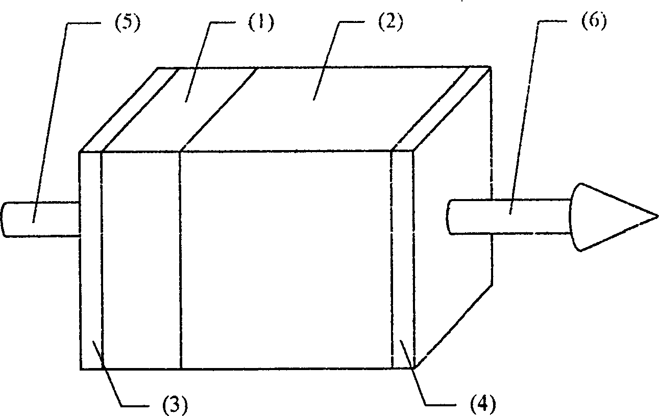
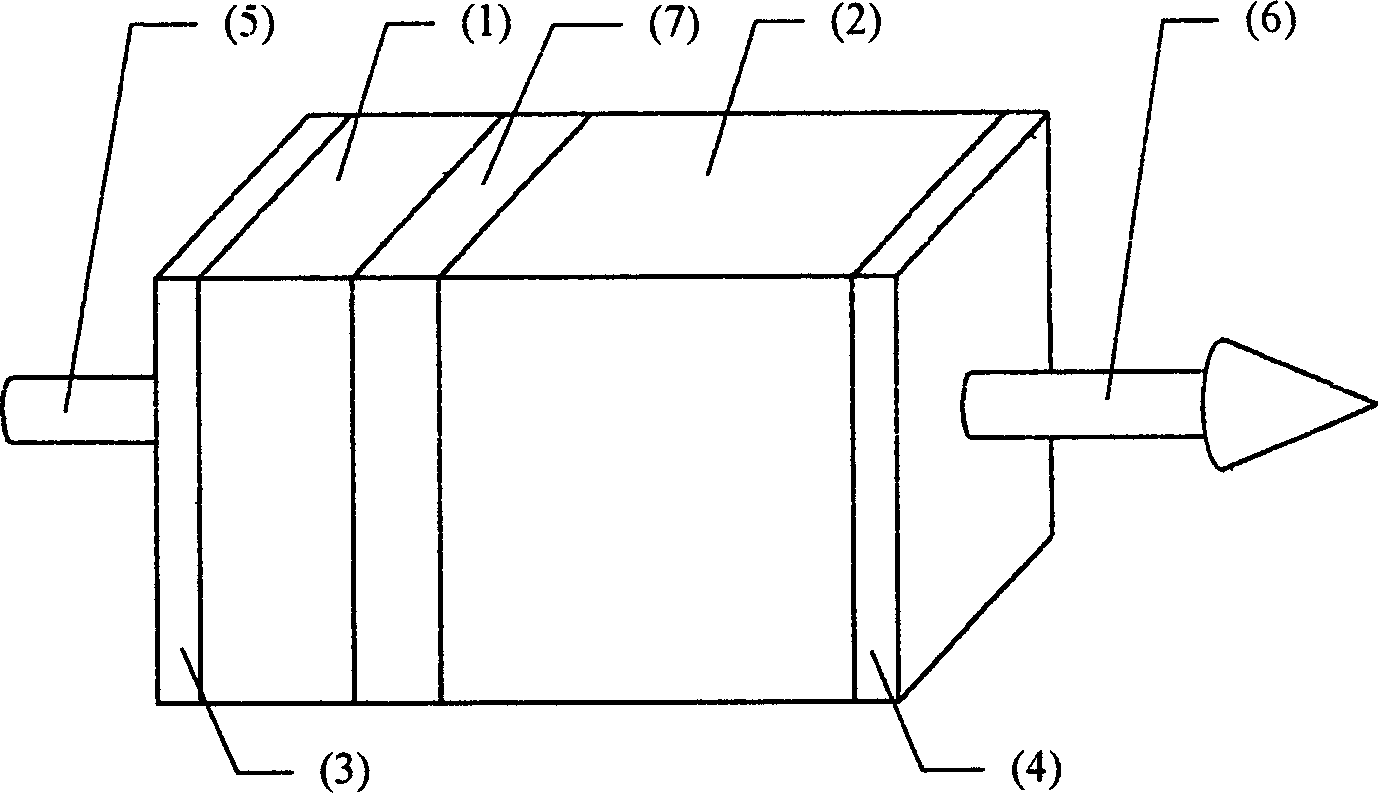
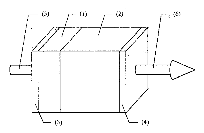
[0021] Example 1: For Nd 3+ ions of 1062 nm ( 4 f 3 / 2 → 4 I 11 / / 2 ) Fundamental wave laser frequency doubling produces 531 nm green laser output. Nonlinear Optical Crystal YAl 3 (BO 3 ) 4 Along the type I phase matching angle θ I =30.7° directional cutting, at the same time determine the size of the crystal (generally a square or cylinder with an end area of ​​mm square and a thickness of several mm), and place the end face in Nd containing flux after polishing x Y 1-x al 3 (BO 3 ) 4 (x is between 0.01 and 1) high temperature flux, using YAl 3 (BO 3 ) 4 As a substrate for liquid phase epitaxy growth, the required thickness of Nd can be obtained on one end face perpendicular to the phase matching direction by controlling the growth time and conditions x Y 1-x al 3 (BO 3 ) 4Crystal microchips. After obtaining the functional crystal in which the above-mentioned laser crystal microchip and the nonlinear optical crystal are integrated, plate the end face 3 as sh...

example 2

[0022] Example 2: For Nd 3+ ion at 1338 nm ( 4 f 3 / 2 → 4 I 13 / 2 ) Fundamental wave laser frequency doubling produces 669 nm red laser output. Nonlinear Optical Crystal YAl 3 (BO 3 ) 4 Along the type I phase matching angle θ I = 27.0° directional cutting, at the same time determine the size of the crystal (generally a square or cylinder with an end area of ​​mm square and a thickness of several mm), and place the end face in Nd containing flux after polishing x Y 1-x al 3 (BO 3 ) 4 (x is between 0.01 and 1) high temperature flux, using YAl 3 (BO 3 ) 4 As a substrate for liquid phase epitaxy growth, the required thickness of Nd can be obtained on one end face perpendicular to the phase matching direction by controlling the growth time and conditions x Y 1-x al 3 (BO 3 ) 4 Crystal microchips. After obtaining the functional crystal in which the above-mentioned laser crystal microchip and nonlinear optical crystal are integrated, plate the end face 3 as shown in...

example 3

[0023] Example 3: Nd 3+ ions of 1062 nm ( 4 f 3 / 2 → 4 I 11 / 2 ) The fundamental wave laser is mixed with the 807 nm semiconductor laser as the pump light to generate a 458 nm blue laser output. Nonlinear Optical Crystal YAl 3 (BO 3 ) 4 Along the type I phase matching angle θ I =35.0° directional cutting, at the same time determine the size of the crystal (generally a square or cylinder with an end area of ​​mm square and a thickness of several mm), and place the end face in Nd containing flux after polishing x Y 1-x al 3 (BO 3 ) 4 (x between 0 and 1) high temperature flux, using YAl 3 (BO 3 ) 4 As a substrate for liquid phase epitaxy growth, the required thickness of Nd can be obtained on one end face perpendicular to the phase matching direction by controlling the growth time and conditions x Y 1-x al 3 (BO 3 ) 4 Crystal microchips. After obtaining the functional crystal in which the above-mentioned laser crystal microchip and the nonlinear optical crystal ...


PUM


Abstract

In one end surface perpendicular to the frequency doubling or frequency mixing phase matching direction of non-linear optical crystal, laser crystal microchip or Q-modulating chip and laser crystal microchip are produced through epitaxial growth, and this realizes integral solid microchip laser with frequency modulation function pumped by semiconductor laser or other proper optical source. The laser can convert the light of semiconductor laser or other proper optical source into visible or UV laser beam.

Description

technical field [0001] The invention relates to crystal material and optoelectronic technology. Background technique [0002] A microchip laser is a small laser with a laser crystal thickness of less than 1 mm and a dielectric film that meets the laser operating conditions directly on both sides. The semiconductor laser can be used as the pump source for end pumping, and the semiconductor laser with poor beam quality and monochromaticity can be converted into a solid-state laser output with high beam quality and good monochromaticity. On this basis, Q-switching elements and nonlinear optical crystals can be added to perform Q-switching, frequency doubling or frequency mixing on the solid-state fundamental wave laser to obtain laser output in the visible and ultraviolet bands. This type of device has the advantages of low pumping threshold, high conversion efficiency, stability and reliability, compact device, and convenient use. It has broad application prospects in the fie...

Claims


Application Information

Patent Timeline
IPC IPC(8): G02F1/35H01S3/10H01S3/16
Inventor 黄艺东陈学元涂朝阳罗遵度
Owner FUJIAN INST OF RES ON THE STRUCTURE OF MATTER CHINESE ACAD OF SCI
Why Eureka
Try Eureka