Method for producing semiconductor apparatus

A semiconductor and device technology, applied in the field of manufacturing semiconductor devices, can solve the problems of multi-layer interconnect leakage current and device misoperation, and achieve the effect of solving leakage current and device misoperation

Inactive Publication Date: 2004-12-22
RENESAS ELECTRONICS CORP
View PDF0 Cites 4 Cited by
  • Summary
  • Abstract
  • Description
  • Claims
  • Application Information

AI Technical Summary

Problems solved by technology

[0020] In order to solve the above-mentioned problems, the present invention has been accomplished, and the object of the present invention is to sufficiently remove the contaminants adhered on the inner walls of through-holes and grooves for burying wiring, thereby solving leakage currents and devices in multilayer interconnections. the problem of misuse

Method used


Image

  • Method for producing semiconductor apparatus
  • Method for producing semiconductor apparatus
  • Method for producing semiconductor apparatus

Examples


example 1

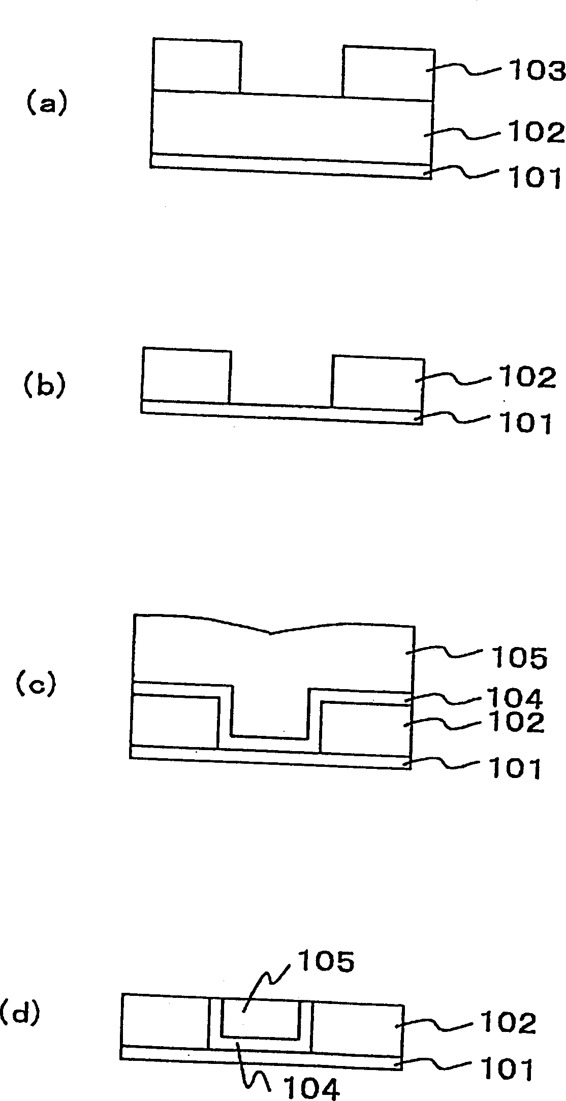
[0068] refer to Figure 1-4 Describe this example. This example employs a damascene interconnection for each of the lower wiring and the upper wiring, and uses a so-called dual damascene process method.

[0069] (Formation of lower wiring)

[0070] First, the lower wiring is fabricated as follows. On a semiconductor substrate (not shown) on which devices such as transistors are formed, a silicon oxide film 101 having a thickness of 100 nm and an HSQ film 102 having a thickness of 400 nm are formed. Next, a photoresist mask 103 with a predetermined pattern is formed thereon [ figure 1 (a)]. Dry etching is performed using this mask to form grooves for burying lower wiring in the HSQ film 102 . Subsequently, the photoresist mask 103 is peeled off by performing ashing with oxygen plasma and cleaning with a cleaning solution containing an amine compound.[ figure 1 (b)].

[0071] Next, on the entire surface of the obtained substrate, a TiN film 104 (thickness: 50 nm) was fo...

example 2

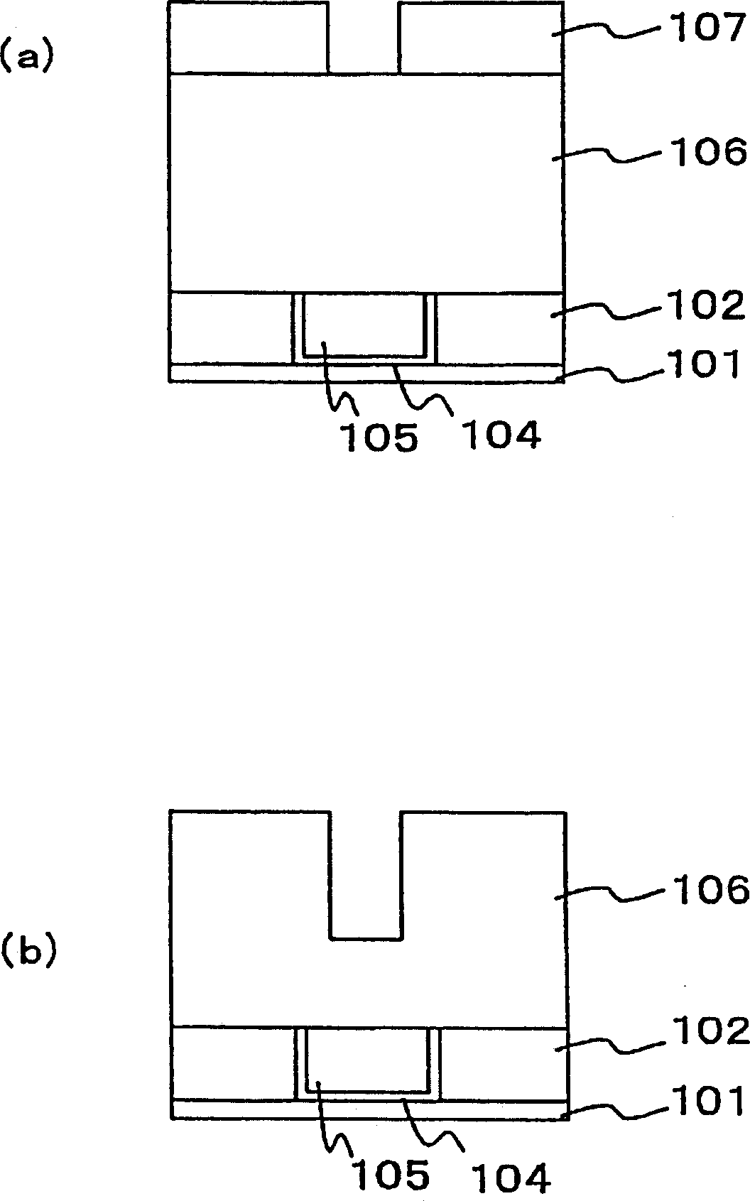
[0080] In this example, a silicon nitride film is formed on the lower wiring, which is used as an etch stopper film when forming a via hole. Thus, it is desired to suppress the lower wiring made of copper and reduce the amount of metal contamination adhering to the inner wall of the via hole. The manufacturing steps will be described below with reference to the drawings.

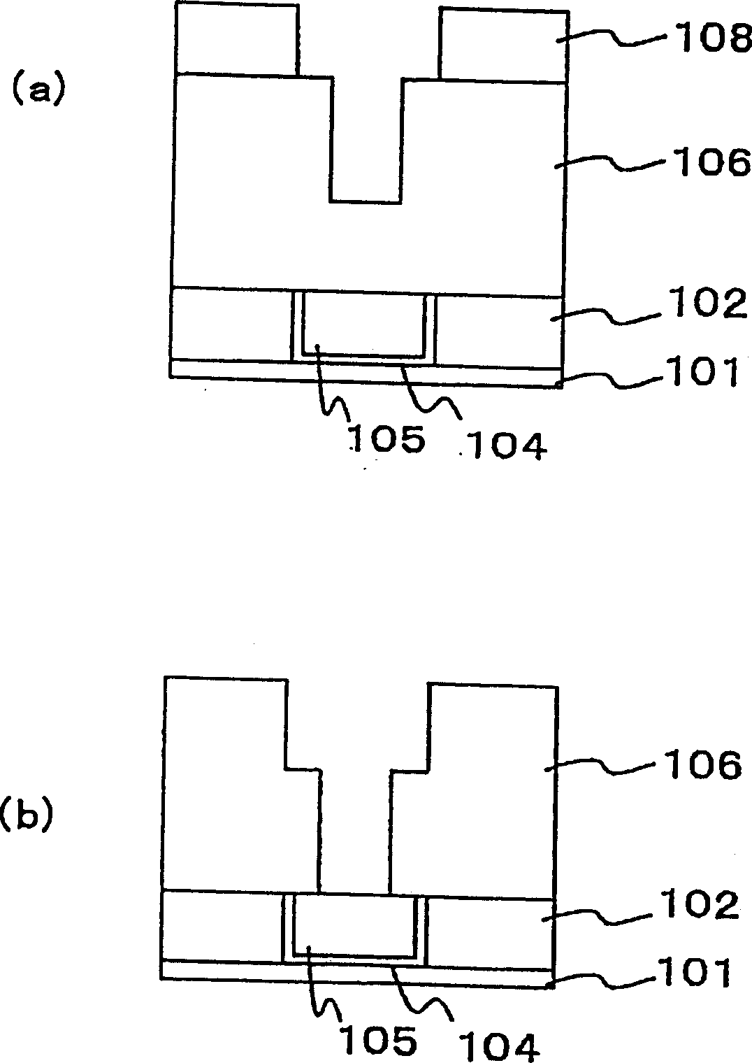
[0081] First, press the figure 1 The same process shown in the form of the lower wiring, as figure 1 (a)-1(d). Then, a silicon nitride film 120 having a thickness of 100 nm is formed thereon by CVD. Furthermore, the HSQ film 106 and the resist film 107 were formed in the same manner as in Example 1 [ Figure 10 (a)]. Each pore diameter of the resist film 107 is 0.25 μm.

[0082] Next, dry etching is performed using this resist mask 107 to form a part of a via hole in the HSQ film 106 . As a corrosive gas, use a 4 f 8 and Ar mixed gas. The dry etching is terminated before the bottom of the via hol...


PUM


Abstract

In a method of manufacturing a semiconductor device having a multi-layer interconnection, after a via hole has been formed, the inside of the via hole is cleaned using a cleaning solution containing a complexing agent capable of forming a complex with contaminants of copper type metals.

Description

technical field [0001] The present invention relates to a manufacturing method of a semiconductor device with multilayer interconnection, wherein the multilayer interconnection connects upper wiring and metal wiring made of copper-like metal material through via holes. Background technique [0002] A representative example of a conventional manufacturing method of a semiconductor device having a multilayer interconnection will be described with reference to FIGS. 5-8. This example is a so-called dual damascene process method in which lower wiring and upper wiring are separately formed so as to have a damascene interconnection. [0003] On a semiconductor substrate (not shown) on which devices such as transistors are formed, a silicon oxide film 201 having a thickness of 100 nm and a HSQ (hydrogen silisesquipoxane )) film 202. Next, a photoresist mask 203 [FIG. 5(a)] with a predetermined pattern is formed thereon. Utilize this mask to carry out dry etching, and form a concav...

Claims


Application Information

Patent Timeline
Patent Type & Authority Patents(China)
IPC IPC(8): H01L21/302H01L21/02H01L21/28H01L21/304H01L21/306H01L21/3205H01L21/768H01L23/52H01L23/522
CPCH01L21/76814H01L21/76813H01L21/02063H01L2924/0002H01L2924/00H01L21/768
Inventor 青木秀充
Owner RENESAS ELECTRONICS CORP
Why Eureka
Try Eureka