
Light-emitting diode

A technology for light-emitting diodes and light-emitting components, which is applied in electrical components, electrical solid-state devices, circuits, etc., can solve the problems of reduced size and lack of brightness, and achieve the effect of increasing brightness and easy control.

Inactive Publication Date: 2005-03-23
TOYODA GOSEI CO LTD +1
View PDF0 Cites 0 Cited by
  • Summary
  • Abstract
  • Description
  • Claims
  • Application Information

AI Technical Summary

Problems solved by technology

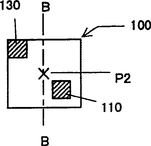
Therefore, if a design is used, the flip chip 100 is placed on the seat 520 so that the central axis of the flip chip 100 coincides with the central axis of the rectangular sub-seat 520, and the above-mentioned exposed portion for connecting electrodes can be guaranteed. , then the size of the flip chip 100 will be reduced; like this, the required brightness may not be obtained

Method used


Image

  • Light-emitting diode
  • Light-emitting diode
  • Light-emitting diode

Examples


Embodiment Construction

[0053] The invention will now be illustrated by specific examples. However, the present invention is not limited to these Examples.

[0054] First, a light emitting diode 1 according to a first embodiment of the present invention shown in FIG. 1 will be described.

[0055] Before explaining the light emitting diode 1, the structure of a flip chip 100 made of gallium nitride compound semiconductor used in this embodiment will be explained. Figure 3A with 3B A cross-sectional view and a plan view of the flip chip 100 are shown, respectively. Reference numeral 101 denotes a sapphire substrate; 102 denotes a buffer layer made of aluminum nitride (AlN); 103 denotes gallium nitride (GaN) which is high in carrier density (Carrier density) doped with silicon (Si) The n-type semiconductor layer of the gallium nitride compound; 104 represents the In x Ga 1-x An active layer made of N (0y Ga 1-y A p-type cladding layer 105 made of N (02 and 130 represent a negative electrode inclu...


PUM


Abstract

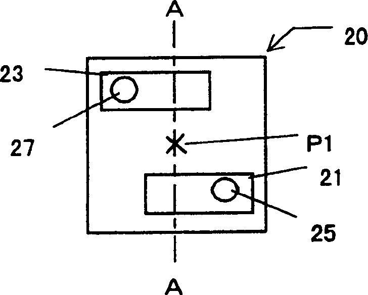
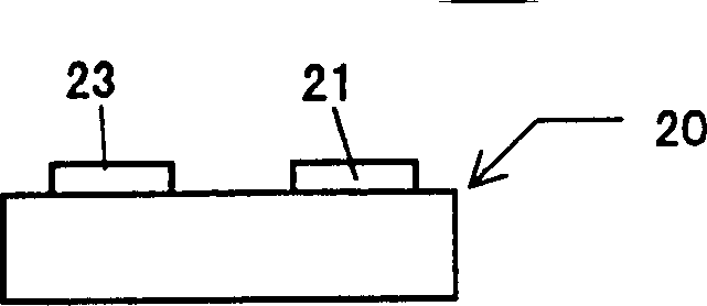
In a light-emitting diode, a substantially square flip chip is placed on a substantially square sub-mount at a position and posture which are obtained through superposition of a center point and center axis of the flip chip on a center point and center axis of the sub-mount and subsequent rotation of the flip chip about the center points by approximately 45°. Therefore, triangular exposed regions are formed on the sub-mount, in which two lead electrodes for the flip chip can be formed. As a result, the flip chip can be placed on a lead frame such that the center axis of the flip chip coincides with the center axis of a parabola of the lead frame. Further, the sub-mount is formed of a semiconductor substrate, and a diode for over-voltage protection is formed within the semiconductor substrate. Therefore, breakage of the light-emitting diode due to excessive voltage can be prevented.

Description

technical field [0001] The present invention relates to a light emitting diode using a flip chip type light emitting element having a wide light emitting surface. Background technique [0002] Referring now to Fig. 12 and Fig. 13, a general light emitting diode 5 using a flip chip type semiconductor light emitting element will be described. FIG. 13 schematically shows a vertical section of the appearance and structure of a general light emitting diode 5 including a flip chip type semiconductor light emitting element 100 (hereinafter referred to as "flip chip 100"). FIG. 12 shows a light emitting element 570, which is composed of a sub-mount 520 as a substrate and a flip chip 100 mounted on the sub-mount. [0003] The lead frame 50 is composed of a metal post 51 and a metal rod 53 for applying voltage to the light emitting element 570 . The metal rod 53 has a reflective portion 55 and a plane portion 54 for placing the light emitting element 570 . A resin cover 40 encloses...

Claims


Application Information

Patent Timeline
IPC IPC(8): H01L33/06H01L33/28H01L33/32H01L33/34H01L33/36H01L33/38H01L33/40H01L33/44H01L33/48H01L33/56H01L33/60H01L33/62
CPCH01L23/62H01L2224/16145H01L2924/10253H01L33/385H01L2224/48257H01L2224/45144H01L2224/48091H01L33/48H01L2224/48247H01L25/167H01L2224/0558H01L2224/05001H01L2224/1703H01L2924/00014H01L2924/00H01L2224/05639H01L2224/05644H01L2224/05673H01L2924/01079H01L2924/013H01L2224/05655H01L2924/01047H01L2224/05657H01L2224/05623H01L2224/05672H01L2224/05613H01L2224/05683H01L2224/05681H01L2224/05181H01L2224/05171H01L2224/05671H01L2224/05684H01L2224/05184H01L2224/05166H01L2224/05666H01L2224/05647H01L2224/05147H01L2224/05164H01L2224/05664H01L2224/05669H01L2224/05169H01L2224/05111H01L2224/05611H01L2224/05624H01L2224/05124H01L2224/05157H01L2224/05123H01L2224/05172H01L2224/05149H01L2224/05649H01L2224/05113H01L2224/05183H01L2224/05118H01L2224/05618H01L2224/0518H01L2224/0568H01L2224/05679H01L2224/05179H01L2224/05139H01L2224/05144H01L2224/05155
Inventor 平野敦雄吉川幸雄手岛圣贵安川武正
Owner TOYODA GOSEI CO LTD
Learn More