Multi-order memory unit

A multi-level storage and polysilicon technology, applied in electrical components, electrical solid-state devices, circuits, etc., can solve the problems of complex peripheral circuits and excessive storage unit size

Inactive Publication Date: 2005-05-25
WINBOND ELECTRONICS CORP
View PDF0 Cites 0 Cited by
  • Summary
  • Abstract
  • Description
  • Claims
  • Application Information

AI Technical Summary

Problems solved by technology

[0005] For traditional multi-level flash memory, because it requires different voltage values ​​for writing, the peripheral circuits required are quite complicated.
And its reliability issues are also different from those of single-unit memory
On the other hand, although the multi-storage flash memory, the reliability and the circuit complexity are similar to the memory of the unit cell, there is a problem that the size of the memory cell is too large

Method used


Image

  • Multi-order memory unit
  • Multi-order memory unit
  • Multi-order memory unit

Examples


Embodiment Construction

[0013] In order to make the above-mentioned purpose, features and advantages of the present invention more obvious and easy to understand, a preferred embodiment is specifically cited below, together with the accompanying drawings, and described in detail as follows:

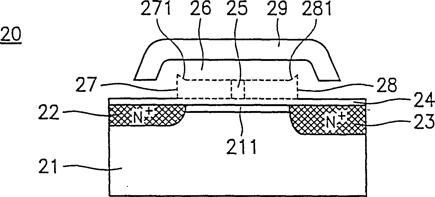
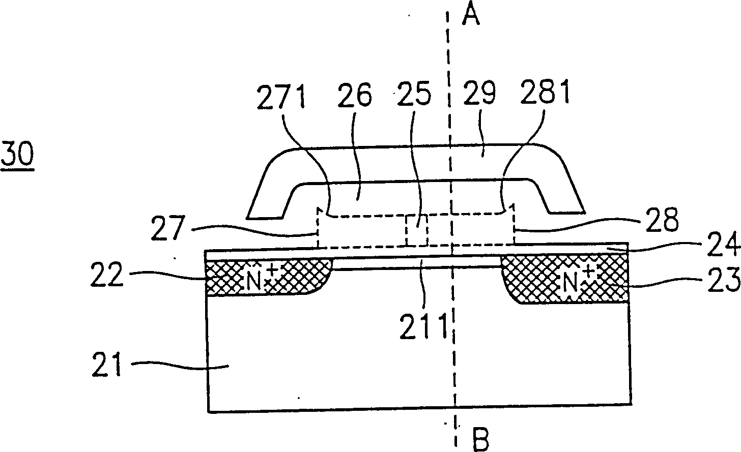
[0014] figure 2 is a cross-sectional view of a multi-level unit 20 according to an embodiment of the present invention. The multi-level memory cell 20 uses an N channel, which has a substrate 21, two doped regions 22, 23 located in the substrate 21 with different doping concentrations and used as source / drain electrodes, a channel region 211, a Gate oxide layer 24 , an insulating layer 25 isolating two floating gates 27 , 28 , a tunnel oxide layer and bird's beak insulating layer 26 , and a control gate 29 . The floating gates 27 and 28 are, for example, polysilicon layers; the insulating layer 25 is, for example, an oxide layer; the bird's beak insulating layer 26 is, for example, a bird's beak oxide layer; a...


PUM


Abstract

The invention provides a multi-level memory unit, which includes a substrate, a first floating gate, a second floating gate and a control gate. The substrate has a first doped region, a second doped region and a channel region located between the first doped region and the second doped region. The first floating gate is insulated on the channel region next to the first doped region. The second floating gate is insulated on the channel region next to the second doped region, and is separated from the first floating gate. The control gate is insulated on the first and second floating gates. When this kind of memory cell writes different bits, the bias voltage value of the control gate is the same, and the first doped region or the second doped region is biased with a fixed voltage value depending on the bit to be stored. In addition, when writing The same bias value is used on the control gate when entering and erasing, so the storage capacity per unit chip area is increased, and the purpose of simplifying the peripheral circuit is also achieved.

Description

technical field [0001] The present invention relates to a semiconductor storage device, in particular to a multi-level storage unit, which can store multiple bits and increase the bit storage capacity per unit chip area without complex peripheral circuits. Background technique [0002] As CMOS technology penetrates below the sub-micron level, the density of flash memory is also increasing, which greatly reduces the cost per bit. However, more problems will be encountered in the process of reducing the size of the circuit. Some researchers have proposed multi-level structures of different types of memory, including DRAM, SDRAM, and Flash EEPROM. Among them, the multi-level Flash EPROM is particularly noticed. Before the concept of the multi-level structure was applied to the flash memory, a flash memory cell could only store one bit, and the reading of the bit was controlled by changing the threshold voltage. The change in the threshold voltage is caused by the change in t...

Claims


Application Information

Patent Timeline
Patent Type & Authority Patents(China)
IPC IPC(8): H01L21/8239H01L27/10
Inventor 林泓均王是琦陈泰元
Owner WINBOND ELECTRONICS CORP
Why Eureka
Try Eureka