Organic EL face-board and making method thereof

An organic and panel technology, applied in semiconductor/solid-state device manufacturing, vacuum evaporation plating, coating, etc., can solve problems such as resistance reduction, performance deterioration, and current increase

Inactive Publication Date: 2006-04-05
SANYO ELECTRIC CO LTD
View PDF0 Cites 0 Cited by
  • Summary
  • Abstract
  • Description
  • Claims
  • Application Information

AI Technical Summary

Problems solved by technology

From this, it can be seen that in this part, the resistance of the electron transport layer decreases and the amount of current increases, and the electron transport layer emits light strongly, causing deterioration in performance.

Method used


Image

  • Organic EL face-board and making method thereof
  • Organic EL face-board and making method thereof
  • Organic EL face-board and making method thereof

Examples


Embodiment Construction

[0021] Embodiments of the present invention will be described below with reference to the drawings.

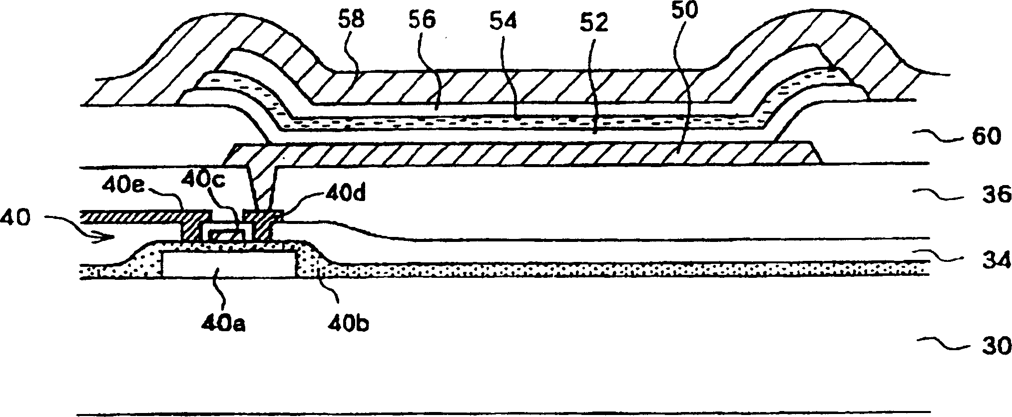
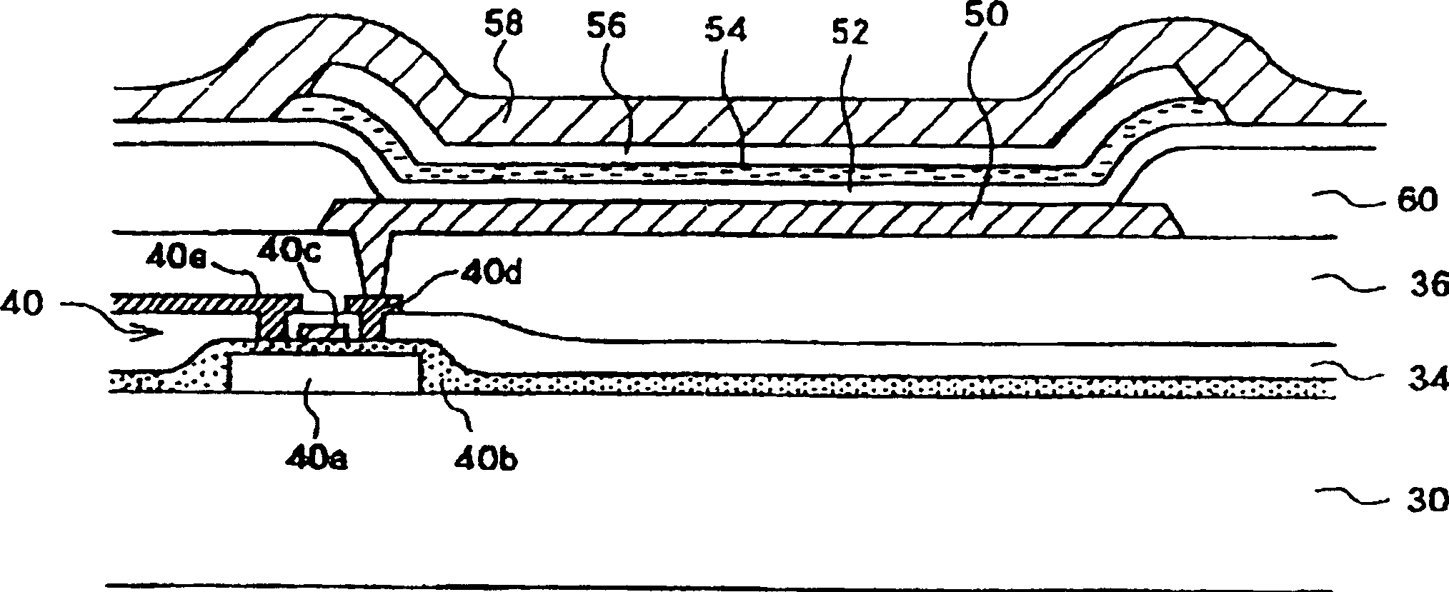
[0022] figure 1 Represents the composition of pixels. Here, two TFTs, one capacitor, and one organic EL element EL are formed in one pixel on the active matrix element substrate, but only the driving TFT 40 and the organic EL element EL are shown in this figure.

[0023] In the drawing, the element substrate has a driving TFT 40 formed on a glass substrate 30 . An organic EL element is connected to this driving TFT 40 .

[0024] The driving TFT 40 is formed on the glass substrate 30 with an active layer 40a formed of low temperature polysilicon. Both ends of the active layer 40 a are source regions and drain regions doped with impurities, and the center of these regions is a channel region. A gate electrode 40c is formed above the channel region via a gate insulating film 40b made of silicon oxide. The gate insulating film 40b and the gate electrode 40c are covered by the...


PUM


Abstract

A second planarization (insulating) film is formed so as to cover the periphery of a pixel electrode. Then, using the same mask, a hole transport layer, an organic emissive layer, and an electron transport layer are sequentially formed. In particular, use of larger anisotropy in evaporation for upper layers results in the upper layers which are smaller than the lower layers. Thus, the lateral side of the lower layer is not covered by the upper layer. This can reduce immixing of dust attributable to use of a mask.

Description

technical field [0001] The present invention relates to an organic EL (ELECTRO LUMINESCENCE, electroluminescent) having at least an organic light-emitting layer, an electron transport layer, etc. Organic EL panel with elements arranged in a matrix and method for manufacturing the same. Background technique [0002] It is known that the organic EL display panel has been used as a flat display panel in the past. This organic EL display panel is different from a liquid crystal display panel (LCD) in that it emits light by itself, so it is expected to become a bright and easy-to-view flat panel display panel. [0003] The organic EL display panel uses organic EL elements as pixels, and arranges them into several matrix-like structures. An organic EL element has a structure in which a hole transport layer, an organic light-emitting layer, an electron transport layer, and a cathode of aluminum or the like are laminated on an anode made of ITO or the like. [0004] Here, in orde...

Claims


Application Information

Patent Timeline
Patent Type & Authority Patents(China)
IPC IPC(8): H05B33/12H05B33/10C23C14/12C23C14/24H01L27/32H01L51/00H01L51/40H01L51/50H01L51/56
CPCH01L51/5048H01L51/0013H01L27/3244H01L51/52H01L51/001H10K59/12H10K71/164H10K71/18H10K50/14H10K50/80H10K50/813H10K50/822H05B33/10
Inventor 西川龙司
Owner SANYO ELECTRIC CO LTD
Why Eureka
Try Eureka