

Method and appts. for ionized sputtering of materials
A technology of ionization and equipment, which is applied in the field of sputtering, can solve the problems of increasing the design of the vacuum chamber, reducing the quality, reducing the uniformity of the operating pressure, and achieving the effect of avoiding reaction and preventing the loss of orientation
- Summary
- Abstract
- Description
- Claims
- Application Information
AI Technical Summary
Problems solved by technology
Method used
Image

Examples
no. 1 example
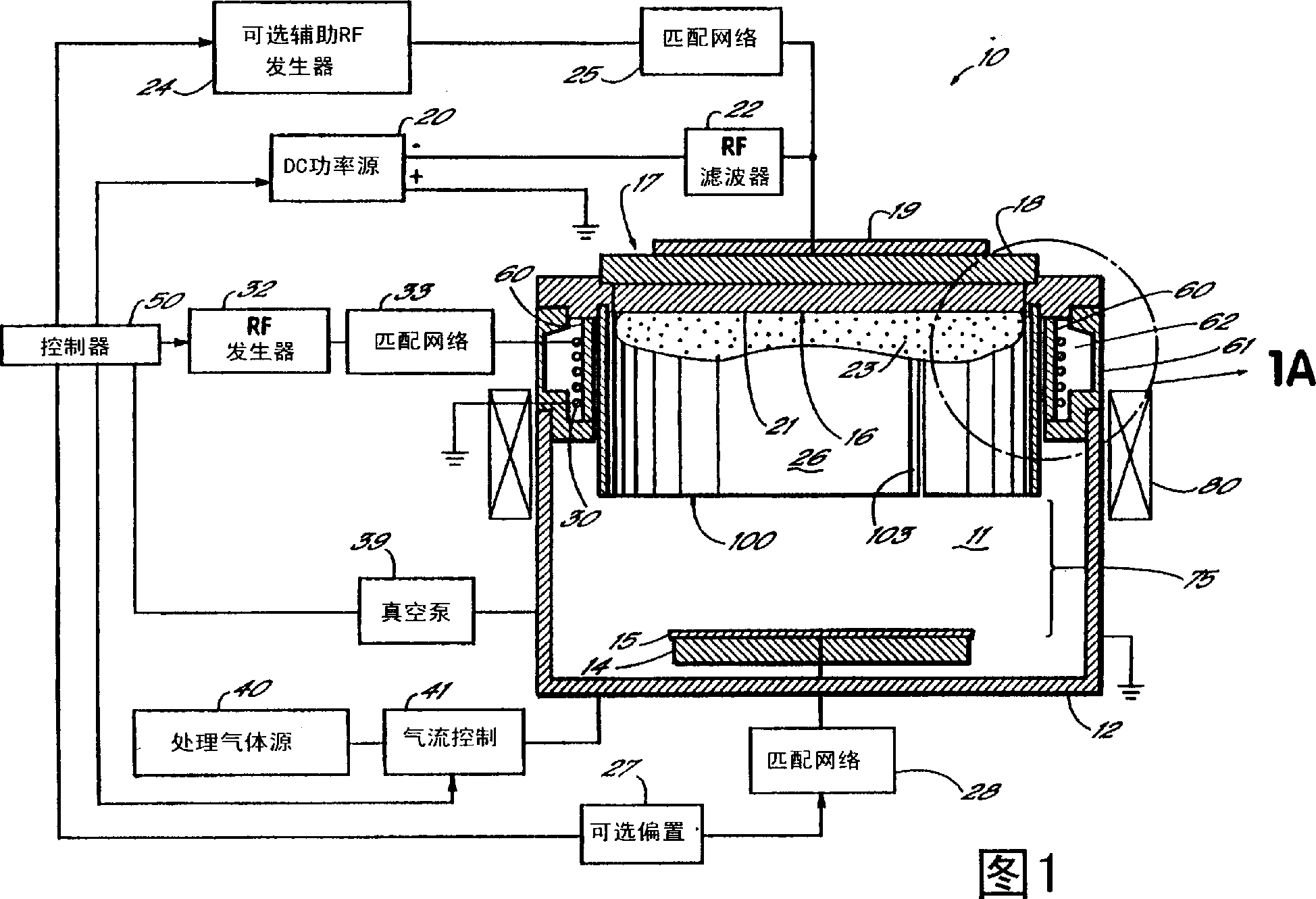
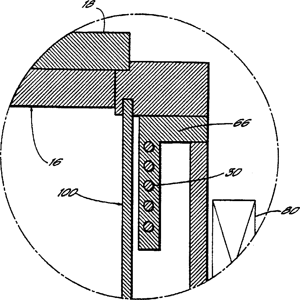
[0020] In a first embodiment, the RF element comprises a helical coil surrounding the chamber from behind a mostly cylindrical quartz window used as a protective structure. This mostly cylindrical quartz windshield may form part of the inner wall of the closed pore of the chamber, or it may be in the form of an insulator surrounding the coil inside the chamber, or some other form of insulating the coil conductors from the process gas.
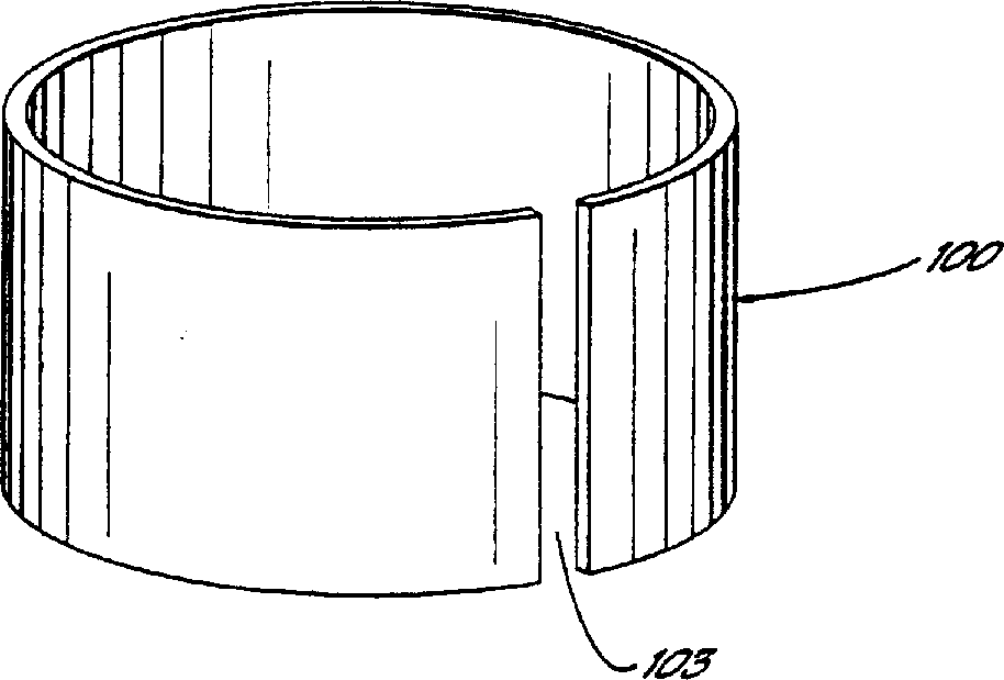
[0021] A substantially cylindrical shield is positioned around the chamber in close proximity to the window separating the coil from the PVD processing chamber. The shield is preferably cut in a direction parallel to the axis of its chamber. By "close proximity" is meant that the distance from the window is short enough to prevent plasma formation between the shield and the window. This cut shield follows the shape of the dielectric window that separates the coil from the vacuum chamber and process gas. This shield prevents deposition of coat...
no. 2 example
[0026] In a second embodiment, an enclosure, a dielectric window, and integral or segmented insulation are used alone or in combination to collectively protect the RF components from the plasma and sputtered material. The shield array is preferably in the form of a plurality of shield segments which can be biased to control their sputtering by the plasma. The shield array has a plurality of gaps to at least partially electrically disconnect shield segments to prevent induced eddy currents from dissipating energy and resist coupling of energy to the plasma. Furthermore, the individual shield subsections are preferably electrically separated so that they can be individually biased to optimize the uniformity of coating on the substrate and the orientation of the ionized material on the substrate. The spacing between the shield segments allows for the transmission of plasma from behind the shield into the processing volume.
PUM
 Abstract
Description
Claims
Application Information