Forming method of oblique inlaid inner connection structure of integrated circuit
An integrated circuit and interconnection technology, applied in the field of dual damascene structure improvement
- Summary
- Abstract
- Description
- Claims
- Application Information
AI Technical Summary
Problems solved by technology
Method used
Image

Examples
Embodiment Construction
[0018] The invention discloses a method for forming a dual damascene interconnect structure. Specifically, the invention provides a method for manufacturing sloped dual damascene interconnect structures and provides an embodiment thereof. The detailed description is as follows, and the preferred embodiments are only for illustration and not for limiting the present invention.
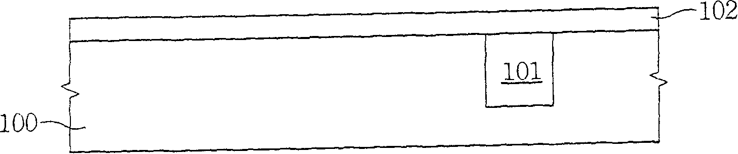
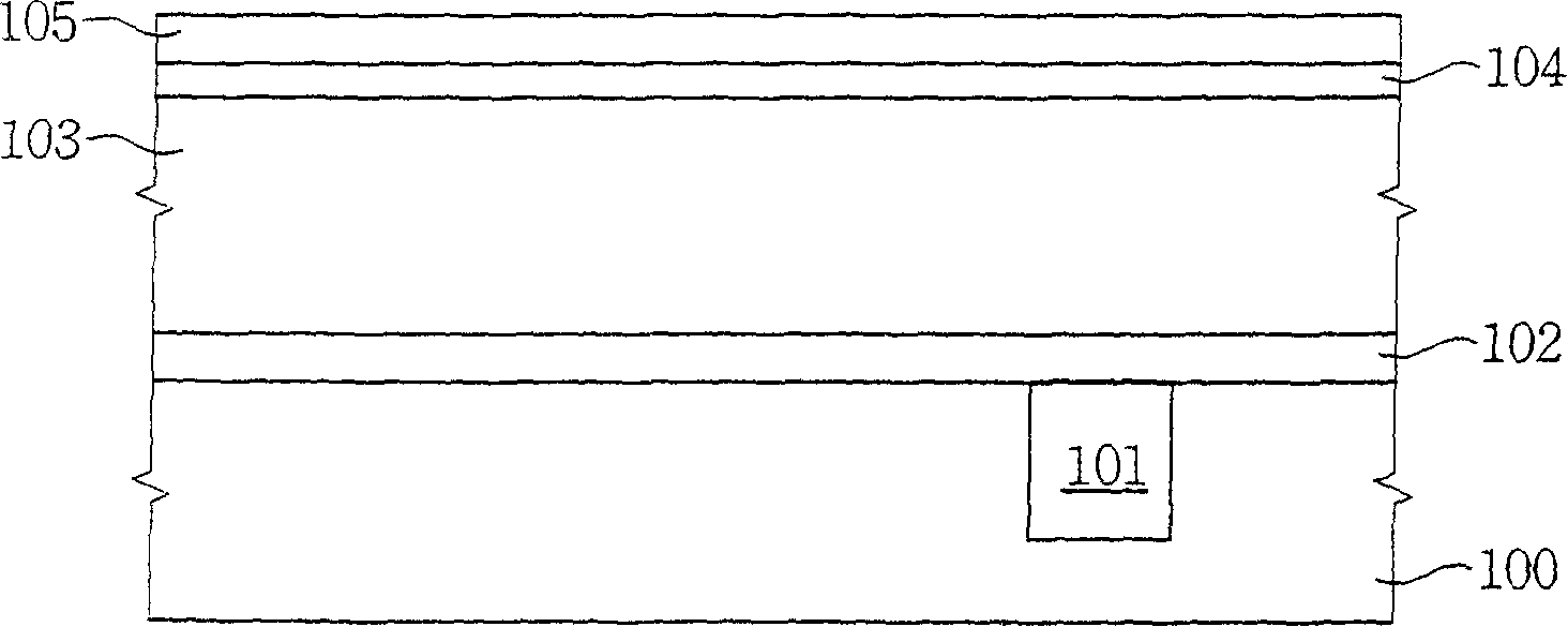
[0019] Please refer to figure 1 , in a preferred embodiment, a structure 100 with a copper plug 101 is provided. Next, a dielectric layer 102 is formed on the copper metal plug 101, and the dielectric layer 102 is a silicon nitride layer formed of silicon nitride. Generally speaking, the above-mentioned silicon nitride layer 102 can be formed by a suitable procedure, such as chemical vapor deposition, at a temperature of about 700 to 1100° C. and in an environment filled with nitrogen. In a specific embodiment, the thickness of the dielectric layer 102 is about 100˜250 angstroms.
[0020] Please refe...
PUM
| Property | Measurement | Unit |
|---|---|---|
| thickness | aaaaa | aaaaa |
| thickness | aaaaa | aaaaa |
| thickness | aaaaa | aaaaa |
Abstract
Description
Claims
Application Information
 - R&D
- Intellectual Property
- Life Sciences
- Materials
- Tech Scout
- Unparalleled Data Quality
- Higher Quality Content
- 60% Fewer Hallucinations
Browse by: Latest US Patents, China's latest patents, Technical Efficacy Thesaurus, Application Domain, Technology Topic, Popular Technical Reports.
© 2025 PatSnap. All rights reserved.Legal|Privacy policy|Modern Slavery Act Transparency Statement|Sitemap|About US| Contact US: help@patsnap.com