Reference voltage generating circuit and voltage amplifier adopting same

A voltage amplifier, reference voltage technology, applied in the direction of amplifiers with semiconductor devices/discharge tubes, DC-coupled DC amplifiers, amplifiers, etc., can solve problems such as large time delays

Inactive Publication Date: 2007-03-07
SOCIONEXT INC
View PDF3 Cites 0 Cited by
  • Summary
  • Abstract
  • Description
  • Claims
  • Application Information

AI Technical Summary

Problems solved by technology

[0008] Also, since the time until the intermediate voltage of the peak value and the valley value is stabilized is the sum of the time for each output of the peak detection and hold circuit and the valley detection and hold circuit to be stable, and the time for the output of the voltage divider circuit to be stable, There is a problem with large time delays

Method used


Image

  • Reference voltage generating circuit and voltage amplifier adopting same
  • Reference voltage generating circuit and voltage amplifier adopting same
  • Reference voltage generating circuit and voltage amplifier adopting same

Examples


no. 1 Embodiment approach

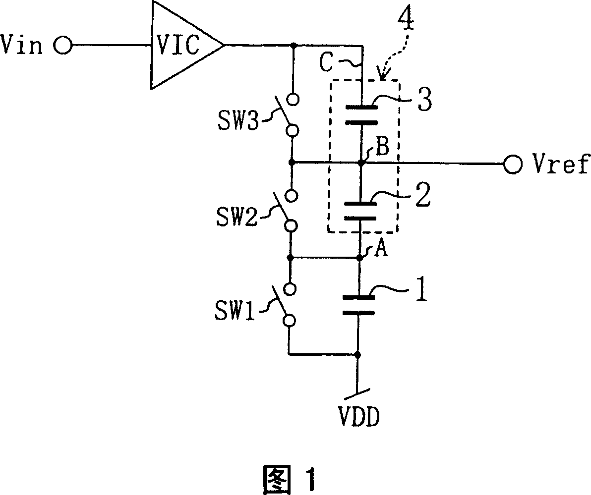
[0073] FIG. 1 shows a reference voltage generating circuit according to the inventions of the inventions 1, 2, 3, 4 and 5 of the first embodiment.

[0074] In this figure, one end of the first capacitor 1 is grounded (here, a given voltage VDD, functioning as a minimum value holding circuit). The other end is connected in series with a capacitor row 4 formed by connecting the second and third capacitors 2 and 3 in series. The switches SW1-SW3 are respectively connected in parallel with the two ends of the capacitors 1-3, and play the role of removing charges. Also, VIC is a voltage-current conversion circuit, which inputs the input voltage signal Vin on its input side, and is connected to the circuit connected in series with the above-mentioned first capacitor 1 and capacitor row 4 on its output side, and its function is until the input voltage Vin is connected to the output Capacitors 1 to 3 are charged (or discharged) until the voltages are equal.

[0075] Hereinafter, the...

no. 2 Embodiment approach

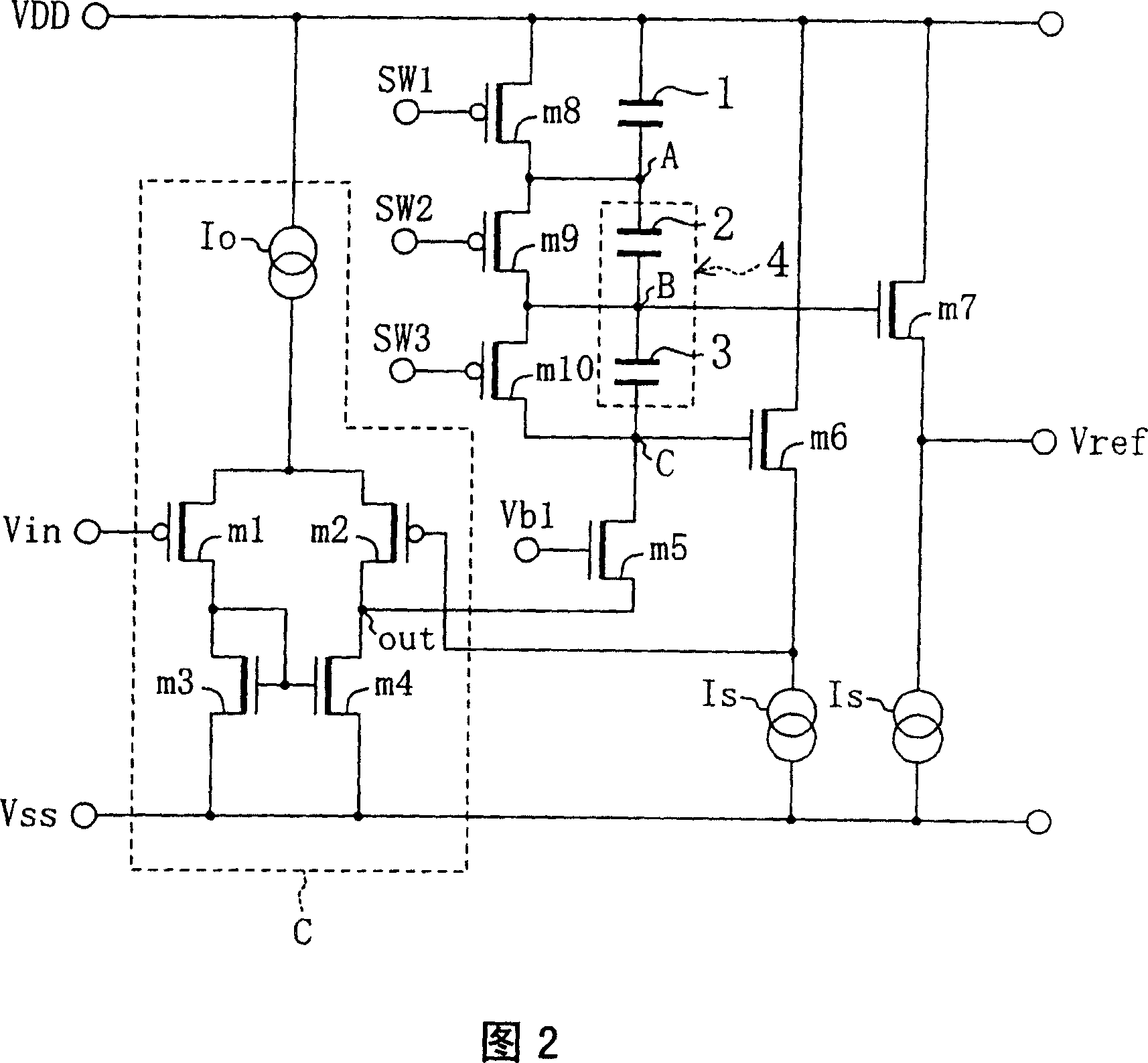
[0097] FIG. 2 shows a reference voltage generating circuit according to the invention described in the sixth embodiment of the present invention.

[0098] The reference voltage generating circuit in FIG. 2 includes a capacitor column 4 and a voltage-current conversion circuit C formed by connecting the first capacitor 1, the second capacitors 2 and the third capacitors 2 and 3 shown in FIG. 1 in series. It further includes a gate-cathode transistor m5 as a unidirectional conduction element that can only pass current in one direction, an NMOS source follower transistor m6 as a buffer circuit, a PMOS transistor m8 as a first reset circuit connected in parallel with the first capacitor 1, PMOS transistors m9 and m10 as a second reset circuit are connected in parallel to the second and third capacitors 2 and 3, respectively.

[0099] The above-mentioned voltage-current conversion circuit C is composed of a differential circuit composed of PMOS transistors m1, m2, NMOS transistors ...

no. 3 Embodiment approach

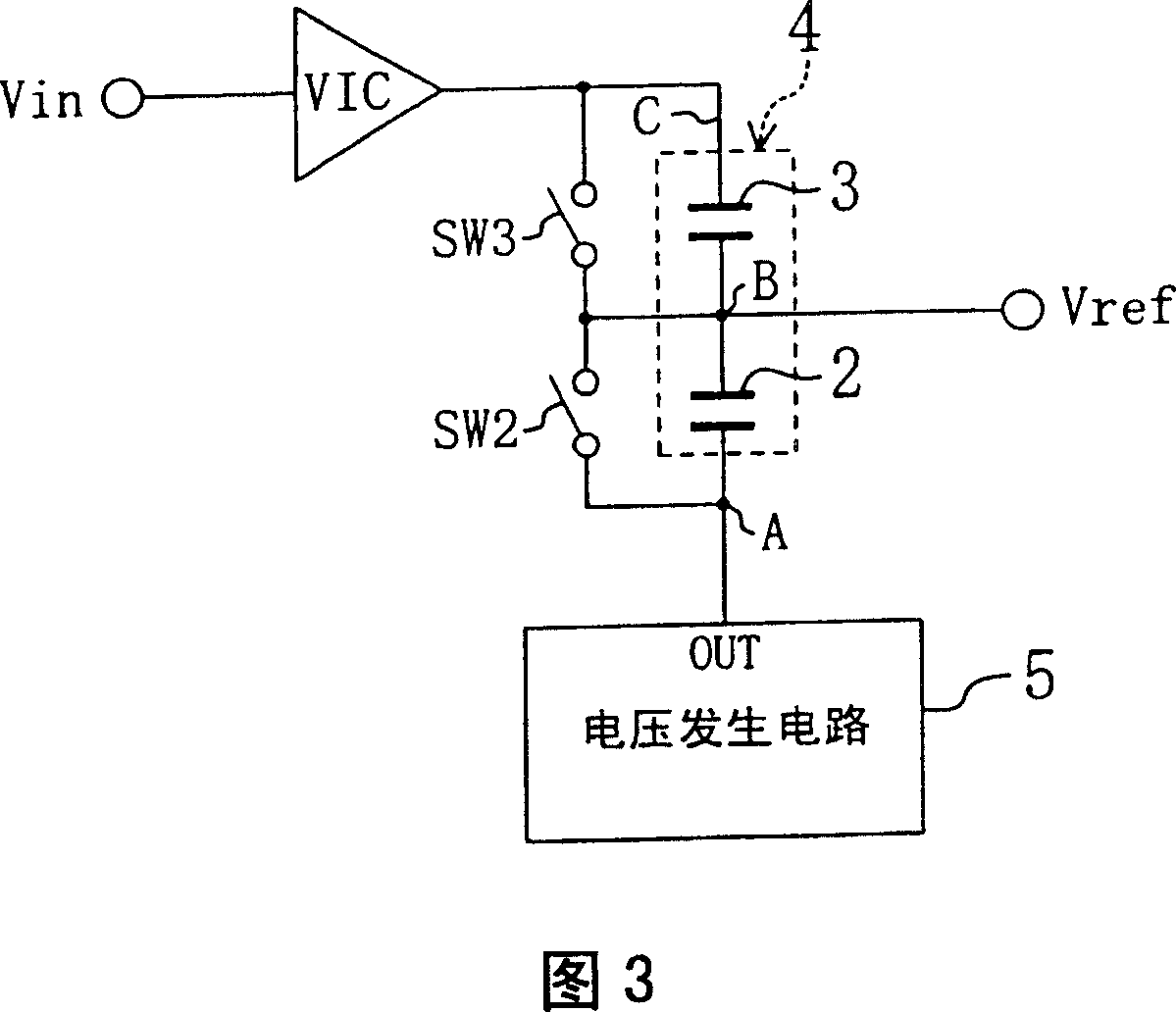
[0105] FIG. 3 shows a reference voltage generating circuit according to inventions 7, 8 and 9 of the present invention according to the third embodiment. In this embodiment, a voltage generating circuit 5 is provided, and this voltage generating circuit 5 is used instead of the first capacitor 1 and the switch SW1 of the first embodiment described above.

[0106] That is, the reference voltage generating circuit in the figure includes a capacitor row 4 formed by connecting two capacitors 2 and 3 in series, two switches SW2 and SW3 connected in parallel to the capacitors 2 and 3, a voltage-current conversion circuit VIC, and A voltage generating circuit 5 that generates a given voltage. An output terminal of the voltage generating circuit 5 is connected to one end of one capacitor 2 of the capacitor array 4 . The voltage at the connection node B of the two capacitors 2 and 3 of the capacitor column 4 is output as a reference voltage Vref. Also in this embodiment, as in the fi...


PUM


Abstract

The invention provides a voltage amplifier that can amplify input signals having a variety of signal amplitudes to a constant amplitude by using the reference voltage generating circuit with excellent high-speed response. In a reference voltage generating circuit, in a first period, only a first switch is OFF and a maximum peak value Vmax of an input signal In is held at a node A of a first capacitor 1. Next, in a second period, a second and a third switches are opened, and a voltage difference between the maximum peak value Vmax and a minimum peak value Vmin is held at a node C of a capacitor string. At this time, the voltage held in a second capacitor of the capacitor string is added to the voltage held in the first capacitor, and the voltage at a node B is output as a reference voltage Vref. The input signal In is applied to one input terminal of a differential amplifying circuit, and the reference voltage Vref is applied to the other input terminal. When the voltages held at the nodes A and C have stabilized, the reference voltage Vref is generated.

Description

technical field [0001] The present invention relates to an optical communication system such as a PDS (Passive Double Star) optical subscriber system, in which current output from a photodiode receiving an optical signal from an optical fiber is converted into a voltage signal, and various signal amplitudes are converted into A voltage amplifier that amplifies the input signal to a certain amplitude. Background technique [0002] Recently, researches on optical joiner systems have been widely carried out for future FTTH (Fiber To The Home). However, introduction of an optical fiber having a large transmission capacity to general households is economically problematic compared with conventional metal wires. Among them, the PDS optical subscriber system, which allows multiple subscribers to perform two-way communication services by branching one optical fiber from the base station side, is expected to solve such economic problems. [0003] In such an optical communication sy...

Claims


Application Information

Patent Timeline
Patent Type & Authority Patents(China)
IPC IPC(8): H03G11/00H03K5/08H03F1/02H03F3/45H03F3/68
CPCH03F3/45762H03F3/45986
Inventor 木村博
Owner SOCIONEXT INC
Why Eureka
Try Eureka