Alignment method and apparatus for array type optical probe scanning IC photoetching system

A technology for scanning integrated circuits and photolithography systems, applied in the field of micro-engineering manufacturing, can solve the problems of inability to write error compensation and low efficiency, and achieve the effects of ensuring quality, improving alignment accuracy, and improving alignment efficiency

Inactive Publication Date: 2002-01-30
TSINGHUA UNIV
View PDF0 Cites 18 Cited by
  • Summary
  • Abstract
  • Description
  • Claims
  • Application Information

AI Technical Summary

Problems solved by technology

The alignment device of the traditional photolithography method adopts a one-time alignment method, which cannot compensate for writing errors; each circuit pattern is aligned separately, and the efficiency is low

Method used


Image

  • Alignment method and apparatus for array type optical probe scanning IC photoetching system
  • Alignment method and apparatus for array type optical probe scanning IC photoetching system
  • Alignment method and apparatus for array type optical probe scanning IC photoetching system

Examples


Embodiment Construction

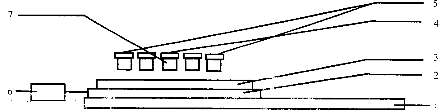
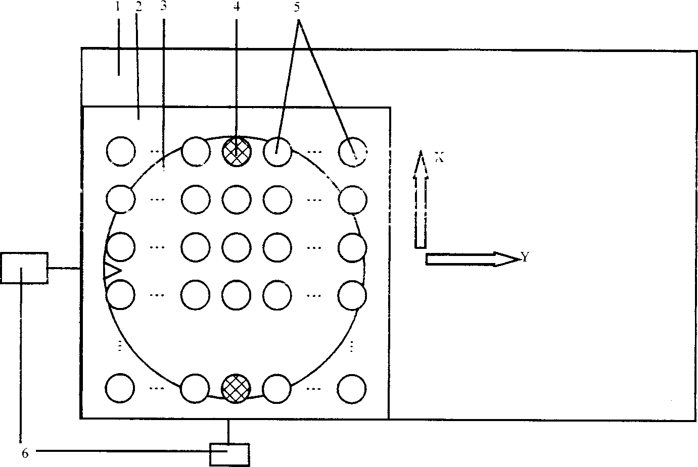
[0022] Such as figure 1 As shown, the alignment device designed in the present invention for array optical probe scanning integrated circuit lithography system includes base 1, work 2, optical probe array 5, calibration optical head 4 and its reading device 7. The workbench 2 is placed on the base 1, driven by the precision servo motor 6, and moves along the X and Y directions. The silicon wafer 3 to be processed is fixed on the workbench 2 through the suction cup, and the calibration optical head 4 and the optical probe array 5 are located on the silicon wafer. Above, a pair of calibration optical heads 4 are located in the middle of the optical probe array 5, which is symmetrical along the Y axis, and the optical probe array 5 is arranged in a rectangular shape. The calibration optical head 4 has a reading device 7 , which includes a light source 51 , a diffusion lens 52 , a polarizing beam splitter 53 , a quarter wave plate 54 , a focusing lens 56 and a photodetector 57 . ...


PUM


Abstract

Firstly, according to the defined key points of circuit pattern, coding distinctive characteristics of circuit pattern, etching them on the silicon wafer, setting a pair a calibrating pattern, makingt he calibrating pattern position at circuit pattern place, and the calibrating pattern is formed from calibrating subpatterns. According to the key points of pattern, on the silicon wafer etching calibrating subpattern, when the alignment is made to key point of pattern, fetching calibrating subpattern coordinate and making comparison of said coordinate with recorded coordinate of calibrating subpattern. In the inveneted equipment the working table is placed on the base seat, and driven by precision servo-actuator, the silicon wafer to be worked can be fixed on the working table by means of suction cup, calibrating optical head and optical probe array are positioned over silicon wafer, a pair of calibrating optical heads is positioned in the middle of optical probe array are positioned over silicon wafer, a pair of calibrating optical heads is positioned in the middle of optical probes, the optcial probes array is arranged in the rectangular form. Said invention can save alignment time of pattern and can raise alignmant efficiency.

Description

technical field [0001] The invention belongs to the field of micro-engineering manufacturing, and is used for the alignment of pattern overlaying in an array optical probe scanning integrated circuit photolithography system. Background technique [0002] Modern large-scale integrated circuit manufacturing mainly adopts photolithography method, coating a layer of photoresist material on the silicon wafer, using optical or electronic exposure to transfer the circuit pattern to the resist, and then developing, etching, etc. A series of processes, and finally get the chip. At present, the line width of large-scale integrated circuits has reached 0.18 μm, and the overlay accuracy is 0.03 μm. [0003] According to the Rayleigh formula R=K×λ / NA, the resolution R depends on the ratio of wavelength to numerical aperture. Traditional optical methods are limited by principles and optical devices, and the resolution is difficult to be less than 0.1 μm, which cannot meet the requiremen...

Claims


Application Information

Patent Timeline
Patent Type & Authority Applications(China)
IPC IPC(8): B81C99/00G03F7/00H01L21/027
Inventor 徐端颐齐国生钱坤李庆祥范晓冬蒋培军
Owner TSINGHUA UNIV
Why Eureka
Try Eureka