

External power supply ring with multiple slender tapes for decreasing voltage drop of integrated circuit
An integrated circuit, narrow and long technology, applied in the direction of circuits, electrical components, electrical solid devices, etc., can solve the problem of more serious voltage drop, increased power consumption and heat generation, and IC cannot operate normally, so as to reduce noise, The effect of reducing the pressure drop
- Summary
- Abstract
- Description
- Claims
- Application Information
AI Technical Summary
Problems solved by technology
Method used
Image

Examples
specific Embodiment approach A
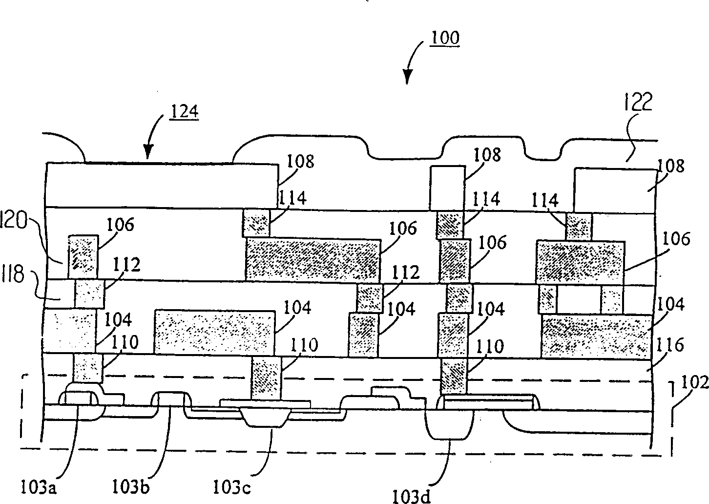
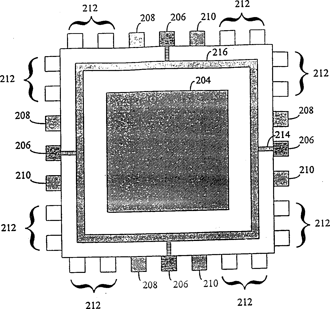
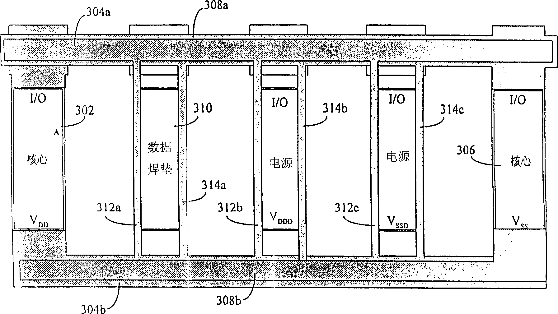
[0047] DETAILED DESCRIPTION OF THE PREFERRED EMBODIMENT A. Development of VLSI Technology
[0048]New processors (sometimes referred to as central processing units (CPUs)) continue to be developed with higher clock frequencies and increased functionality. For example, the reduced instruction set computing (Reduced Instruction Set Computing, RISC for short) architecture will increase the complexity of the interconnection and packaging system due to the input / output (I / O) timing problem caused by the high operating clock frequency. Nowadays, Dynamic Random Access Memory (DRAM) devices, Static Random Access Memory (SRAM) devices, and Electrically Programmable Read-Only Memory (EPROM) The development trend of devices with increased storage capacity and reduced data access time keeps pace with the rapid development of microprocessors. We can say that these microprocessor and memory requirements are the driving force behind IC device technology. The rate at which these new IC devi...
PUM
 Abstract
Description
Claims
Application Information