Method of raising photoetching resolution

A lithography resolution and lithography technology, applied in the direction of micro-lithography exposure equipment, optics, optical components, etc., can solve the problems that affect the formation of fine graphics, limit the improvement of lithography resolution, and affect the quality of lithography graphics. Achieve the effects of large exposure threshold range, improved lithographic line width, and improved lithographic line width

Inactive Publication Date: 2002-10-23
SHANGHAI INST OF OPTICS & FINE MECHANICS CHINESE ACAD OF SCI
View PDF0 Cites 9 Cited by
  • Summary
  • Abstract
  • Description
  • Claims
  • Application Information

AI Technical Summary

Problems solved by technology

[0005] When the photolithographic resolution reaches or even lower than the wavelength of the parallel laser beam G, even if the thickness a of the air gap 103 and the thickness z of the air layer gap 2 are very small, the diffraction effect produced by them also greatly limits the photolithographic resolution The improvement of the influence on the formation of fine graphics
Simultaneously, if there are defects on the surface of the chromium film 102, such as burrs, flaws, small deformations or inclinations, etc., it will directly affect the quality of the photolithography patterns that can be formed on the photoresist layer 3 on the silicon wafer 4.

Method used


Image

  • Method of raising photoetching resolution
  • Method of raising photoetching resolution
  • Method of raising photoetching resolution

Examples


Embodiment Construction

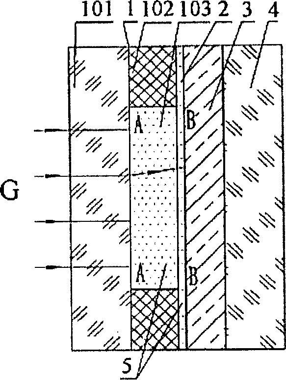
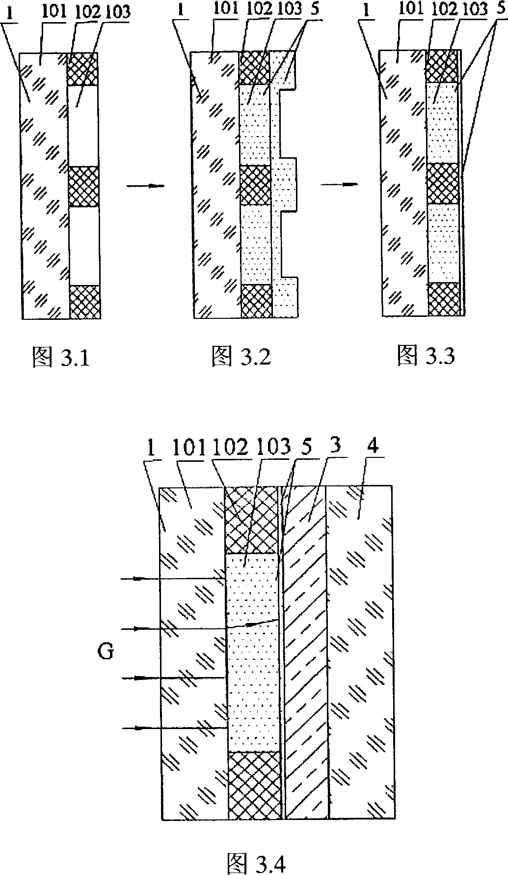
[0027] Such as figure 2 As shown, the wavelength λ of the parallel laser beam G is 157nm, and PMMA photoresist is used as the filled transparent material 5 . Refractive index n of PMMA photoresist at 157nm wavelength t = 1.7226. The thickness a of the chromium film 102 and the transparent material 5 is 47nm, and the width is 0.2 μm. The thickness z of the transparent material 5 in the air gap 2 between the surface of the chromium film 102 and the photoresist layer 3 on the surface of the silicon wafer 4 is 157nm.

[0028] When the parallel laser beam G passes through the mask plate 1 to expose the photoresist layer 3, the exposure amount is 2.6J / cm 2, using a mixture of methyl isobutyl ketone and isopropanol as a developer, the volume ratio of the two is 2:1, and the developing time is 2 min. After development, clear photoresist lines better than 0.20 μm are obtained on the photoresist layer 3 on the surface of the silicon wafer 4 . If the transparent material 5 is not fi...


PUM

PropertyMeasurementUnit
refractive indexaaaaaaaaaa

Abstract

The method for raising photoetching resolution is characterized by that in the air gap being in chrome film pattern on the masket plate photoetched by adopting closing or contact mode and in the air layer space between masked plate chrome film and photoresist layer on the silicon chip a transparent material whose refractivity is greater than that of masked plate is filled, and the surface of saidtransparent material layer which is positioned in air layer space and contacted with photoresist layer is polished, so that when it is photoetched, the transparent material is filled, therefore the refracted angle of light beam is reduced, diffraction distance is reduced, diffraction effect can be effectively weakened to raise the photoetching resolution.

Description

Technical field: [0001] The invention is a method for improving photolithography resolution. Mask plates for proximity / contact lithography. Background technique: [0002] Proximity / contact lithography is the most economical means of producing small batches of ASICs. Common proximity / contact lithography such as figure 1 Shown (referring to the prior art: the paper published by S. Rice et al. in the laboratory of International Business Machines Corporation (IBM) in Applied Physics A, Volume 33, pp. 195-198, 1984). The mask plate 1 is composed of a substrate 101 and a chromium film 102 attached to the substrate 101. The chromium film 102 does not completely cover the surface of the substrate 101. There is a light-transmitting air gap 103 between adjacent chromium films 102. That is, the chromium film 102 forms a pattern on the surface of the substrate 101 . Its working process is: the parallel laser beam G is first incident on the mask plate 1, then passes through the air g...

Claims


Application Information

Patent Timeline
Patent Type & Authority Applications(China)
IPC IPC(8): G02B27/12G03F7/20
Inventor 赵永凯黄惠杰任冰燕杜龙龙程兆谷路敦武杨良民
Owner SHANGHAI INST OF OPTICS & FINE MECHANICS CHINESE ACAD OF SCI
Why Eureka
Try Eureka