Light guide and mfg. method thereof

A manufacturing method and optical waveguide technology, applied in the direction of optical waveguide light guide, coupling of optical waveguide, light guide, etc., can solve the problems of low productivity, lower S/N ratio, lower pass rate, etc., achieve high batch productivity, improve S /N ratio, the effect of speeding up the spreading speed

Inactive Publication Date: 2003-04-16
ORMON CORP
View PDF3 Cites 12 Cited by
  • Summary
  • Abstract
  • Description
  • Claims
  • Application Information

AI Technical Summary

Problems solved by technology

[0008] First of all, the former method of cutting off the core material after the core material is cured has such a problem: since the refractive index of the cladding plate and the waveguide core is not too large, it is difficult to distinguish the interface between the waveguide core and the cladding plate, and it is not easy to determine Where should the waveguide core be cut?
In addition, if the waveguide core is cut off at once by grinding, there may be a possibility that the excess part of the core material cannot be completely removed or the thickness of the cladding plate varies due to differences in the coating thickness of the coated core material and the thickness of the cladding plate. When the cladding board is cut through
Moreover, if the excess part of the core material remains, it will not be possible to prevent light leakage and lower the yield. In addition, once the cladding plate is cut off, the core size of the waveguide will change, and it will become an optical waveguide with different characteristics.
On the other hand, if the waveguide core is cut off with special care, it will take time and effort, and the productivity will be low, leading to problems of increased production cost.
[0009] Secondly, the problem with the latter method of scraping off the waveguide core in an uncured state before the core material is cured is that it is difficult to completely remove the uncured core material with a rubber scraper or the like, and it is extremely easy to scrape off the excess core material anyway. wood residues on cladding panels
Moreover, once a part of the excess core material remains, the light cannot be enclosed in the waveguide core, resulting in a decline in the yield
In addition, when the excess core material is completely scraped off with a rubber scraper, etc., the surface of the core material will be in a concave state due to the surface tension of the core material. When the core material is cured in this state, there will be pits on the surface of the waveguide core. Remains, as a result, the light sealing property deteriorates, the S / N ratio decreases, and it becomes different characteristics, resulting in a decrease in yield

Method used


Image

  • Light guide and mfg. method thereof
  • Light guide and mfg. method thereof
  • Light guide and mfg. method thereof

Examples


no. 2 approach

[0119] Figure 11 (a)(b)(c)(d) are cross-sectional views illustrating a method of manufacturing the optical waveguide 15 according to another embodiment of the present invention. This is implemented, for example, by image 3 The process will have the cladding plate 2 of groove 3, flat part 5, pit 6 to make ( Figure 11 (a)) Afterwards, UV-curable transparent resin 8 is dripped onto the clad plate 2 ( Figure 11 (b)). Next, press the transparent resin 8 on the cladding plate 2 with the die 13, so that the transparent resin 8 is filled in the groove 3, at the same time, the transparent resin 8 on the flat part 5 is extended and thinned, and the excess transparent resin 8 rows to pit 6 side ( Figure 11 (c)). Apply a predetermined pressure to make the film thickness of the transparent resin 8 between the flat part 5 and the stamper 13 a desired film thickness, and after a predetermined time passes, press the transparent resin 8 from the back side of the cladding plate 2 It ...

no. 4 approach

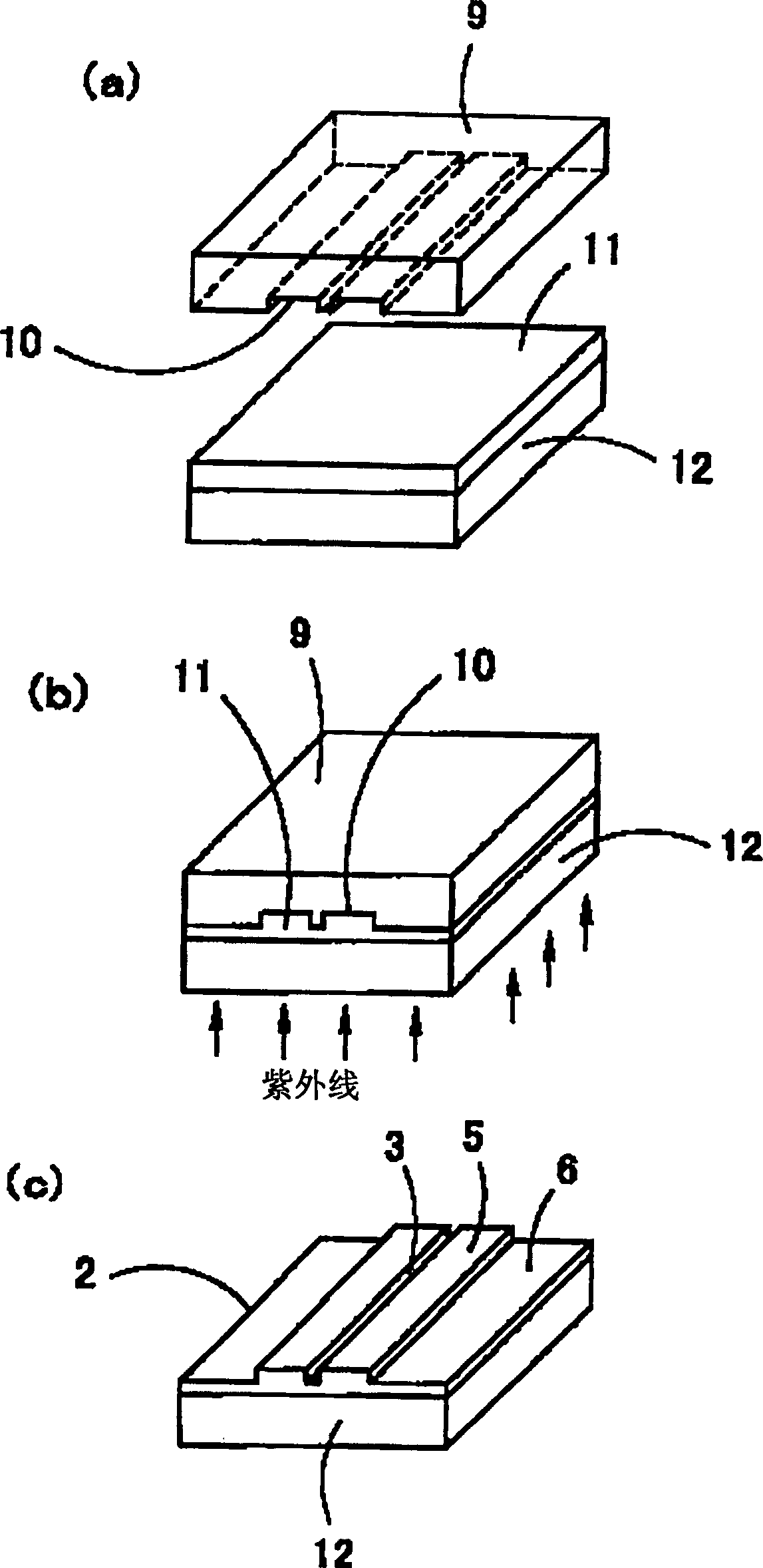
[0122] Figure 13 (a) (b) (c) (d) (e) (f) are cross-sectional views illustrating a method of manufacturing the optical waveguide 17 according to yet another embodiment of the present invention. In this embodiment, the transparent resin 11 ( Figure 13 (a)), by irradiating ultraviolet rays to the transparent resin 11, the clad plate 2 is formed on the upper surface of the glass plate 12 ( Figure 13 (b)). Grooves 3 , flats 5 and dimples 6 are formed on the upper surface of the cladding plate 2 . Then, ultraviolet curing type transparent resin 8 is dropped on this cladding board 2 ( Figure 13 (c)). Next, press the transparent resin 8 on the cladding plate 2 with the die 13, so that the transparent resin 8 is filled in the groove 3, at the same time, the transparent resin 8 on the flat part 5 is extended and thinned, and the excess transparent resin 8 rows to pit 6 side ( Figure 13 (d)). Then, a predetermined pressure is applied to make the film thickness of the transpar...

no. 5 approach

[0124] Figure 14 (a) (b) (c) (d) are cross-sectional views illustrating a method of manufacturing the optical waveguide 18 according to still another embodiment of the present invention. This implementation is, as Figure 14 As shown in (a), in the first cladding plate 2 after manufacture, a triangle is formed between the groove 3 and the dimple 6, and the upper end thereof becomes a pointed portion 19, and the flat portion 5 is not formed. After dripping the ultraviolet curable transparent resin 8 on the cladding board 2 ( Figure 14 (b)), press the transparent resin 8 on the cladding plate 2 with the press die 13, so that the transparent resin 8 is filled in the groove 3. At the same time, the tip portions 19 on both sides of the groove 3 are flattened by the pressing force of the die 13 to form flat portions 5 on both sides of the groove 3 . And, the transparent resin 8 on the flat portion 5 is extended and thinned, and the excess transparent resin 8 is discharged to th...


PUM


Abstract

The present invention provides an optical wave guide that may be produced by reproduction method in easy and simple manner, and has a structure that prevents light signal in its inside from leaking out from core, and a method for producing the same optical wave guide. A concave slot 3 for forming a core is formed on the upper surface of a cladding substrate 2. And on both sides of the concave slot 3, cavities 6 are formed via flat portions 5. An ultraviolet ray hardening type transparent resin 8 is applied onto the surface of the cladding substrate 2, thereafter the transparent resin 8 is pressed by a stamper 13. At this moment, a core 4 is formed in the concave slot 3 and excessive transparent resin 8 pressed between the stamper 13 and the flat portions 5 flows into cavities 6, as a result, it is possible to make the transparent resin 8 thin in a short time. Thereby, it is possible to make the transparent resin 8 left on the flat portions 5 into thickness and width enough to prevent light in the core 4 from leaking out.

Description

[0001] technology area [0002] The present invention relates to optical waveguides and methods for their manufacture. In particular, it relates to the preparation of optical waveguides by molding and methods for their manufacture. Background technique [0003] A conventional optical waveguide is made of quartz, and a waveguide core, cladding, etc. are formed on the quartz by ion implantation or ion exchange. Since the manufacturing process requires a semiconductor manufacturing process using expensive equipment and devices, the cost is high. [0004] For this reason, attempts are also being made to reduce the cost of the optical waveguide by producing the optical waveguide using a replication method (or called a molding method). The simplest low-cost method in the replication method is to apply the core material (transparent resin) only on the surface of the cladding plate that is formed as the groove of the optical waveguide core by pressing, or to press the coated core ma...

Claims


Application Information

Patent Timeline
Patent Type & Authority Applications(China)
IPC IPC(8): G02B6/13G02B6/12G02B6/122G02B6/138G02B6/30G02B6/34G02B6/42G02B6/43
CPCG02B6/43G02B6/1221G02B6/4249G02B2006/1215G02B6/4214G02B2006/12119G02B6/12009G02B6/12004G02B6/138G02B6/30G02B6/4246G02B6/12
Inventor 樋口诚良高桥敏幸户谷浩巳安田成留细川速美佐藤文彦
Owner ORMON CORP
Why Eureka
Try Eureka