Digital circuit implementation by means of parallel sequencers

A sequencer and parallel processing technology, applied in CAD circuit design, electrical digital data processing, combination of multiple digital computers, etc., can solve problems such as difficult to use, bulky, and slow design tools

Inactive Publication Date: 2003-06-04
斯坦利 M 海杜克
View PDF1 Cites 8 Cited by
  • Summary
  • Abstract
  • Description
  • Claims
  • Application Information

AI Technical Summary

Problems solved by technology

However, the fault is not with the design tools, but with the way digital circuits are implemented in silicon
Current silicon architectures make design tools unnecessarily slow, cumbersome and difficult to use

Method used


Image

  • Digital circuit implementation by means of parallel sequencers
  • Digital circuit implementation by means of parallel sequencers
  • Digital circuit implementation by means of parallel sequencers

Examples


Embodiment Construction

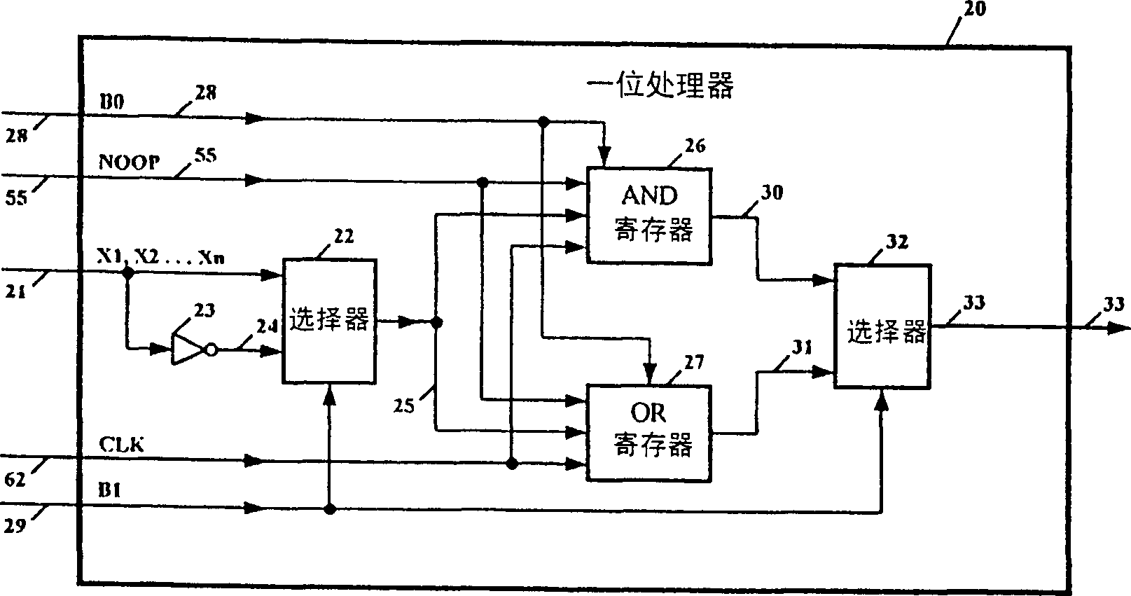
[0032] figure 1 represents an embodiment of a one-bit processor. This embodiment facilitates the execution of Reverse Polish Notation (RPN) machine instructions. Processor 20 is based on two (2) parallel operations performed on all input variables in parallel. figure 1 By way of example, they are shown as AND register 26 and OR register 27 in . Since processor 20 allows an inversion operation by means of inverter 23, the simultaneous presence of registers 26 and 27 does not enforce the logic equation, since the inversion theorem (de Morgan theorem) allows AND The operation is converted to an OR operation or vice versa. It is also within the scope of the present invention to replace the AND register 26 or replace the OR register 27 with a block that performs an XOR or other logical operation.

[0033] At the beginning of the execution of each logic equation, the AND register 26 is set to logic "1". The first "0" resets register 26 to "0" and keeps it at "0" regardless of s...


PUM


Abstract

A system for designing and implementing digital integrated circuits utilizing a set of synchronized sequencers that permit quick and efficient parallel processing of system level designs. The system and method converts digital schematics and hardware description language (HDL) based designs into a set of logic equations and single bit arithmetic-logic operations executed by a set of parallel operating sequencers. The system includes software for converting netlists and DHL designs into Boolean logic equations, and a compiler for distributing these logic equations between multiple sequencers. Each sequencer is comprised of a logic processor and the associated program memory for storing the executable code of the assigned Boolean logic equations and data memory for storing the results of processing of logic equations. To synchronize execution of logic equations by multiple sequencers, all program memories are addressed by one common address register. The processing of logic equations is arranged in such a manner that their outputs can be read by synchronized read instructions in the interconnected sequencers, eliminating any need for control signals.

Description

field of invention [0001] The present invention relates to digital circuit implementation, and more particularly to a new silicon device architecture capable of quickly and efficiently designing and implementing digital integrated circuits. Background of the invention [0002] The realization technology of silicon digital integrated circuit has been very perfect. Numerous technologies such as application-specific integrated circuits (ASICs), field-programmable gate arrays (FPGAs), and synthetic programmable logic devices (CPLDs) exist to implement digital circuits with interconnected elements such as gates, flip-flops, and other digital elements ). The greatest advantage of these technologies is the fast operation due to the parallel action of all digital components. [0003] However, current technology suffers from a number of disadvantages that become more pronounced as component geometries shrink and design sizes increase. For example, the arrangement and routing time ...

Claims


Application Information

Patent Timeline
Patent Type & Authority Applications(China)
IPC IPC(8): G06F15/80G06F17/50
CPCG06F17/5045G06F15/8007G06F17/5022G06F30/30G06F30/33G06F15/16G06F30/3308
Inventor 斯坦利·M·海杜克
Owner 斯坦利 M 海杜克
Why Eureka
Try Eureka