


Quick Research
Generate reliable direction feasibility study reports for your R&D in just a few steps.

Technical Q&A
Discover and master advanced knowledge NOW. Basics, ideas, possibilities, all at once.

Find Solutions
As an expert in R&D theories, this can generate solutions to your technical problems instantly.

Evaluate Feasibility
Analyze your overall solution with one click, know your potential R&D risks in advance.

Monitor Landscape
Get weekly tech updates, stay abreast of the latest tech innovations and key insights.
Random programmable non-volatile semi-conductor storage
A semiconductor and memory technology, applied in the field of non-volatile semiconductor memory, can solve problems such as power consumption, reliability problems, slow speed, etc., and achieve the effects of saving power, improving performance, and shortening access time
- Summary
- Abstract
- Description
- Claims
- Application Information
AI Technical Summary
Problems solved by technology
Method used
Image

Examples
Embodiment Construction
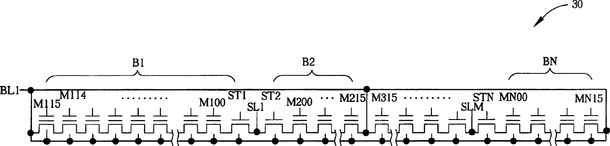
[0028] Please refer to FIG. 2 . FIG. 2 is an equivalent circuit diagram of the NAND non-volatile semiconductor memory 30 of the present invention. As shown in FIG. 2, the NAND memory string block B includes a plurality of rewritable memory cells (memory cell) M, and they are connected in series along the direction of the bit line (bit line) BL1 . Moreover, one end of the memory cell connected in series is electrically connected to the bit line BL1, and a selecting transistor ST is provided at the other end of the memory cell connected in series, and is electrically connected to a source line SL.
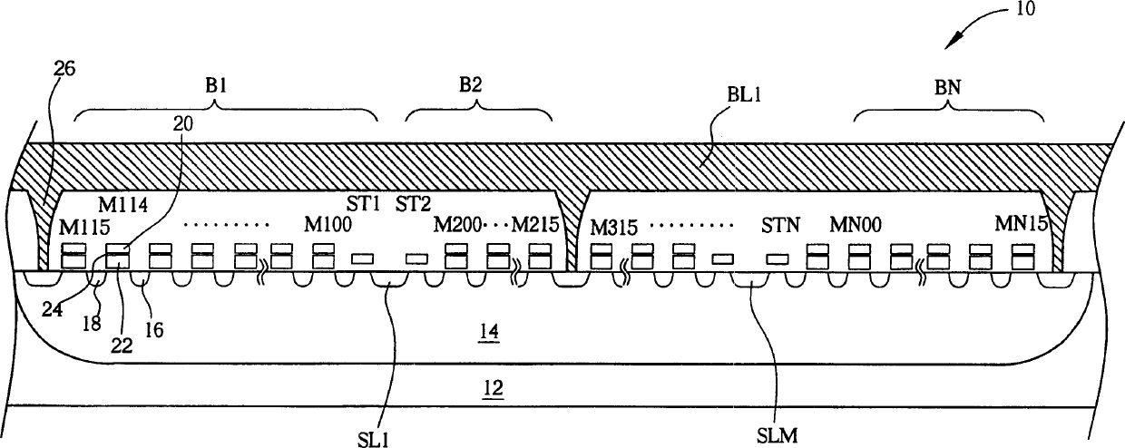
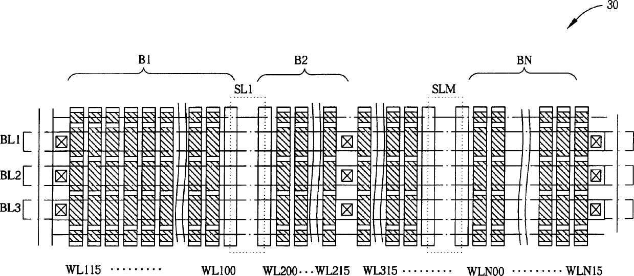
[0029] Please refer to FIG. 3 and FIG. 4 . FIG. 3 is a layout diagram of the NAND non-volatile semiconductor memory 30 of the present invention. FIG. 4 is a cross-sectional view of the NAND non-volatile semiconductor memory 30 along the bit line BL1 in FIG. 3 . As shown in Fig. 3 and Fig. 4, NAND type non-volatile semiconductor memory 30 comprises a first conductive type semiconduc...
PUM
 Abstract
Description
Claims
Application Information
 - R&D Engineer
- R&D Manager
- IP Professional
- Industry Leading Data Capabilities
- Powerful AI technology
- Patent DNA Extraction
Browse by: Latest US Patents, China's latest patents, Technical Efficacy Thesaurus, Application Domain, Technology Topic, Popular Technical Reports.
© 2024 PatSnap. All rights reserved.Legal|Privacy policy|Modern Slavery Act Transparency Statement|Sitemap|About US| Contact US: help@patsnap.com