Shalow groove isolation manufacturing method for preventing acute angle
A technology of shallow trench isolation and manufacturing method, which is applied in the field of shallow trench isolation manufacturing and can solve the problems of complicated manufacturing process and the like
- Summary
- Abstract
- Description
- Claims
- Application Information
AI Technical Summary
Problems solved by technology
Method used
Image

Examples
Embodiment Construction
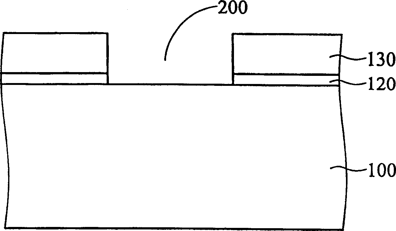
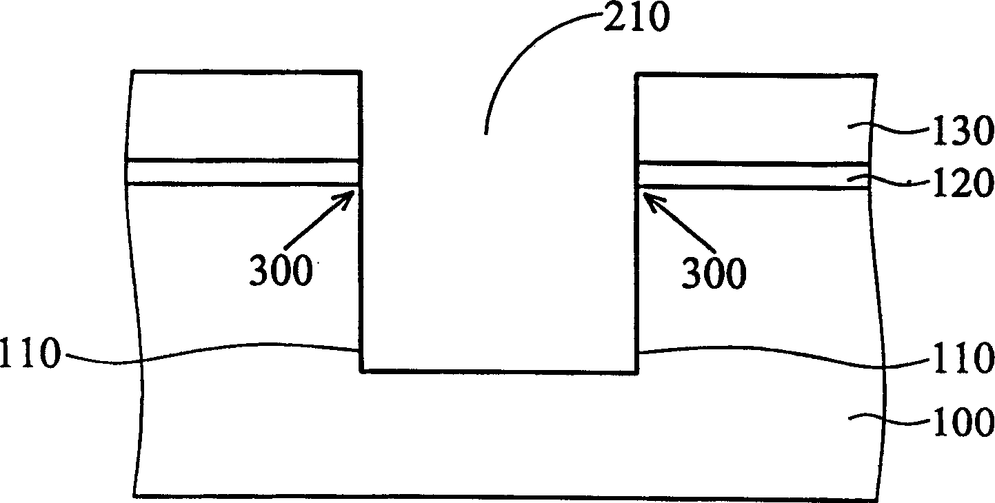
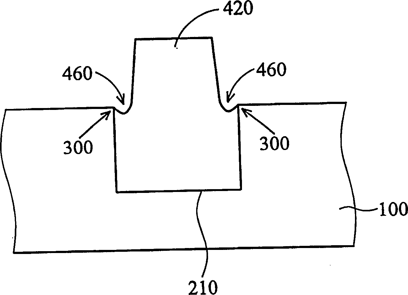
[0047] Figures 2a to 2e A schematic cross-sectional view of a manufacturing method for manufacturing a shallow trench (STI) structure that avoids sharp angles according to a preferred embodiment of the present invention.
[0048] see Figure 2a A silicon oxynitride (SiON; silicon oxynitride) layer 12 and a masking layer 13 are sequentially formed on a semiconductor substrate 10 . The semiconductor substrate is, for example, a silicon substrate. The formation method of SiON layer 12 is: for example, using SiH 4 , N 2 O, N 2 As a reactive gas, it is formed by low pressure chemical vapor deposition (LPCVD; low pressure chemical vapor deposition) or plasma-assisted chemical vapor deposition (PECVD; plasma-enhanced chemical vapor deposition), and the thickness can be between 150 Å and 250 Å . The shielding layer 13 can be a silicon nitride layer, and dichlorosilane (SiCl 2 h 2 , dichlorosilane) and NH 3 It is a reactive gas, formed by LPCVD method, and the thickness can b...
PUM
 Abstract
Description
Claims
Application Information