
Distributing base board and electronic device using it

A technology of wiring substrates and insulating substrates, which is applied to circuits, printed circuits, electrical components, etc., and can solve problems such as current leakage and short circuits

Inactive Publication Date: 2003-12-10
HITACHI LTD
View PDF1 Cites 4 Cited by
  • Summary
  • Abstract
  • Description
  • Claims
  • Application Information

AI Technical Summary

Problems solved by technology

As a result, deterioration phenomena called current leakage and short circuit occur between wiring

Method used


Image

  • Distributing base board and electronic device using it
  • Distributing base board and electronic device using it
  • Distributing base board and electronic device using it

Examples


Embodiment 1

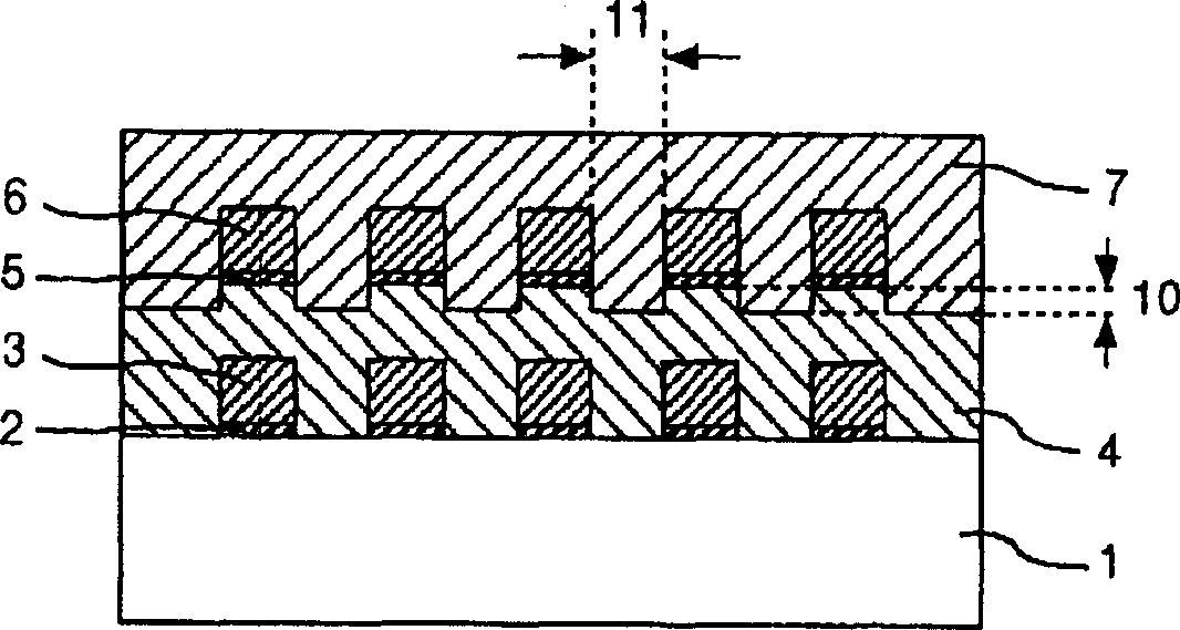
[0066] figure 1 is a schematic cross-sectional view of the wiring board of this embodiment. The upper part of the insulating resin layer 4 located on the metal conductor (wiring) space 11 is formed lower than the surface connecting the lower surface of the base layer 5 and the upper surface of the insulating layer 4, and the protective insulating layer 7 is formed thereon.

[0067] That is, the interface between the insulating resin layer 4 and the protective insulating layer 7 on the metal conductor (wiring) space 11 is located at a position lower than the surface where the base metal layer 5 and the insulating resin layer 4 are connected by a height difference of 10.

[0068] Figure 13 The purpose is to form the upper part of the insulating resin layer 4 located between the metal conductors 11 lower than the surface where the base metal layer 5 and the insulating resin layer 4 are connected. Figure 12 An additional step diagram added after step (k) of the conventional m...

Embodiment 2

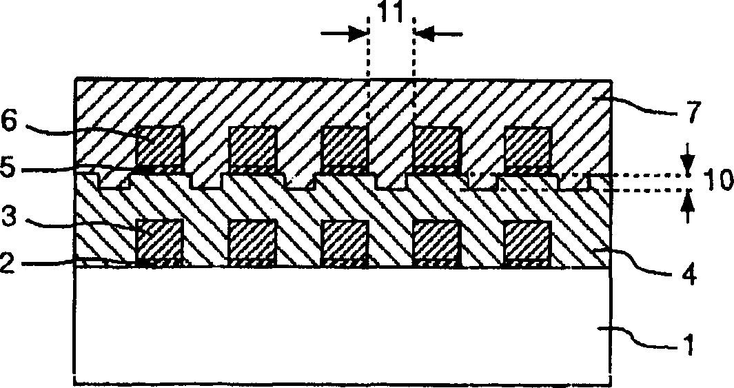
[0073] figure 2 is a schematic cross-sectional view of the wiring board of this embodiment. The central portion of the insulating resin layer 4 located between the metal conductors 11 is removed by ion beam processing to form a protective insulating layer 7 lower than the connection surface between the base metal layer 5 and the insulating resin layer 4 .

[0074] Part of the interface between the insulating resin layer 4 and the protective insulating layer 7 located on the metal conductor (wiring) space 11 is located at a position lower than the surface where the base metal layer 5 and the insulating resin layer 4 are connected by a height difference of 10. Also, the height of the step 10 is about 500 nm.

Embodiment 3

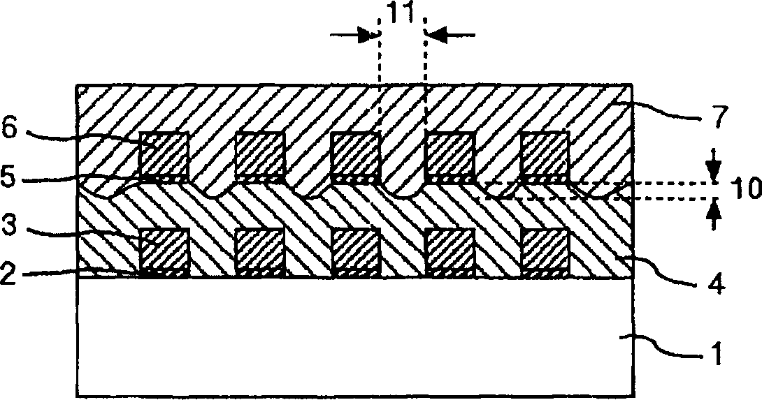
[0076] image 3 is a schematic cross-sectional view of the wiring board of this embodiment. The upper surface of the central portion of the insulating resin layer 4 located on the metal-conductor space 11 is removed by laser processing to form a concave shape. The bottom of this concave portion is formed lower than the surface where base metal layer 5 and insulating resin layer 4 are connected, and protective insulating layer 7 is formed thereon.

[0077] The recessed interface between the insulating resin layer 4 and the protective insulating layer 7 located on the metal conductor (wiring) space 11 is located only 10 steps lower than the surface where the base metal layer 5 and the insulating resin layer 4 are connected. Also, the height of the step 10 is about 1 μm.


PUM


Abstract

The present invention provides a printed wiring board which has high insulation resistance between wirings and is unlikely to cause failures such as leakages or short circuits, attributable to ion migration even in high temperatures and highly humid environments. The printed wiring board has a circuit comprising a metal conductor on base metal layers created by forming an insulating resin layer 4 on at least one face of an insulating substrate 1 and forming the base metal layers 2 and 5 on the insulating resin layer. In the printed wiring board, at least a part of an upper face of the insulating resin layer existing in spaces 11 between the metal conductors is formed at a position lower than the interface between the base metal layer 5 and the insulating resin layer 4.

Description

technical field [0001] The present invention relates to electronic devices such as a wiring board, a semiconductor device using the same, and a multi-chip module. Background technique [0002] In recent years, electronic devices such as mobile phones, portable information terminals, notebook personal computers, digital cameras, video cameras, etc. have been increasingly reduced in size, weight, and performance. As a result, it is used in semiconductor devices such as BGA (ball grid array) / CSP (chip size package) that use this wiring board to fix and support their electronic components, wiring boards that form circuits, and multi-chip modules. Further densification is also required. [0003] In order to cope with this increase in density, composite substrates, glass substrates, etc. have been proposed and put into practical use. [0004] As an example of these wiring boards, Figure 9 A schematic cross-sectional view showing a wiring board in which a two-layer wiring patter...

Claims


Application Information

Patent Timeline
Patent Type & Authority Applications(China)
IPC IPC(8): H01L23/12H01L23/498H05K3/00H05K3/10H05K3/18H05K3/22H05K3/46
CPCH05K3/184H01L2924/19105H05K3/0023H05K3/108H01L24/48H01L2924/01079H05K3/22H01L2224/48227H01L2924/01019H01L2924/15311H05K2201/09045H01L2924/01078H01L23/49822H01L2224/48228H05K3/0041H05K2201/09036H05K3/4644H01L2924/19041H01L2224/16225H01L2224/48091H01L2224/451H01L2924/00014H01L2924/12042H01L2924/14H01L2924/181H01L2924/00H01L2224/05599H01L2924/00012H01L2224/45099H01L2224/45015H01L2924/207H05K1/02H01L23/12
Inventor 楠川順平武内良三
Owner HITACHI LTD
Learn More