Semiconductor device with high structure reliability and low parasitic capacitance

A semiconductor and device technology, applied in the field of semiconductor devices, can solve the problems of reducing mechanical strength, damaging the semiconductor area, and reducing the pass rate, so as to achieve the effect of easy alignment margin and avoiding crack damage

Inactive Publication Date: 2004-02-11
HITACHI LTD
View PDF0 Cites 9 Cited by
  • Summary
  • Abstract
  • Description
  • Claims
  • Application Information

AI Technical Summary

Problems solved by technology

[0005] However, as described above, when mesa etching is performed for device isolation in the structure of prior art 1, in the backside etching step of forming a via hole from the backside inside the transistor region to arrange the conductive region of the emitter electrode, if the via If the hole and mesa corrosion area are not strictly aligned, the yield will be reduced
Moreover, when a large alignment margin is used in order to avoid reducing the yield, the chip area increases, resulting in an increase in chip cost
[0006] Although prior art 2 does not require the electrode contact area to be set within the transistor area, the trench on the back side is made larger, and the area of ​​the thin area of ​​several microns increases, which may reduce the mechanical strength
[0007] Moreover, in both the prior art 1 and the prior art 2, an organic adhesive such as epoxy paste is used for bonding on the chip bonding, and a solvent is generated in the through hole due to heating and drying of the adhesive. vapor, so the pressure inside the via increases, sometimes damaging the semiconductor region on the via
[0008] And, this will result in a structure where a thin semiconductor layer of a maximum of several μm or less is left near the electrode contact region, for example, the stress applied to the chip bonding due to the increased pressure in the via hole is concentrated in the thin Semiconductor regions, causing crystallization to crack, expand until transistor regions fail due to chip damage or transistor damage

Method used


Image

  • Semiconductor device with high structure reliability and low parasitic capacitance
  • Semiconductor device with high structure reliability and low parasitic capacitance
  • Semiconductor device with high structure reliability and low parasitic capacitance

Examples


Embodiment 1

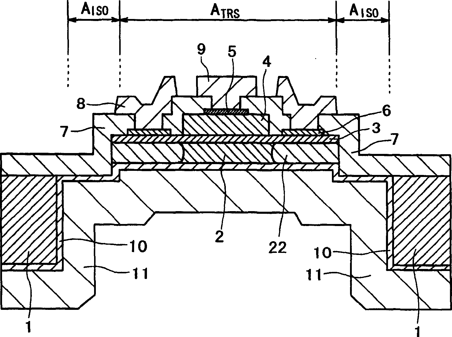
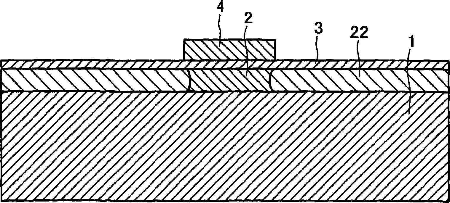
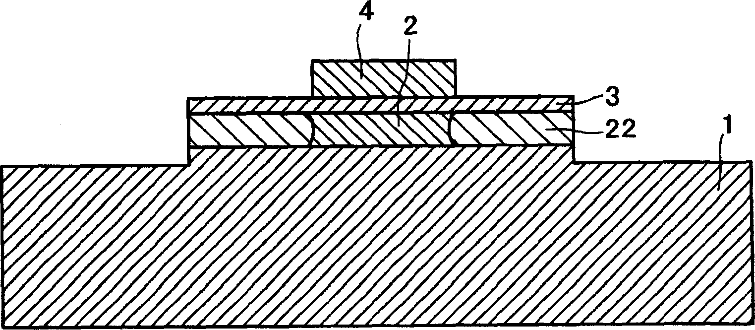
[0036] figure 1 An example of the semiconductor device according to the first embodiment of the present invention is shown. figure 1 The semi-insulating GaAs substrate 1, the emitter layer 2, the base layer 3, the collector layer 4, the collector electrode 5, the base electrode 6, the SiO 2 Surface protective insulating film 7, base wiring metal 8, collector wiring metal 9, emitter electrode 10, emitter wiring metal 11, and emitter damaged region 22 are formed on the entire back surface. figure 1 Medium, A TRS is the transistor region occupied by the emitter layer 2 . Transistor area A TRS A damaged area 22 is also included.

[0037] In this embodiment, the opening of the via from the back to the substrate 1 is larger than the transistor region A TRS , the emitter region 2 and the substrate 1 are isolated and connected by the surface protection insulating film 7 , the emitter electrode 10 and the emitter wiring metal 11 .

[0038] Below, refer to the attached Figure 2 ...

Embodiment 2

[0064] Figure 10 is a schematic cross-sectional structure diagram of a semiconductor device according to this embodiment. The difference from Embodiment 1 above is that during the crystal growth in step (1), an InGaP emitter contact layer 30 is provided between the GaAs substrate 1 and the emitter layer 2, and this layer is doped until the electron concentration reaches 5 ×10 18 cm -3 , a GaAs collector contact layer 20 is provided on the collector layer 4, which is doped until the electron concentration also reaches 5×10 18 cm -3 . The process of manufacturing a transistor was performed in the same manner as in Example 1.

[0065] Due to the provision of highly doped contact layers 20 and 30, the emitter and collector resistances are reduced, i.e. for a collector size of 2×20 μm 2 For the device, the collector resistance is reduced from 10Ω to 2.5Ω, and the emitter resistance is reduced from 20Ω to 4Ω. Thus, the cut-off frequency of the device is increased to 20GHz-30...

Embodiment 3

[0067] FIG. 11 shows a schematic cross-sectional structure of the semiconductor device of this embodiment. It differs from Embodiment 1 above in that the emitter layer 2, the base layer 3, and the collector layer 4 are arranged in the reverse order so that the emitter is on the upper side during the crystal growth in step (1). That is, an upper emitter type transistor is formed. The process of manufacturing a transistor was performed in the same manner as in Example 1.

[0068] Due to the upper emitter type, only the emitter mesa area A E The part directly below forms the active region of the transistor, so there is no need to increase the resistance of the passive region through ion implantation, which can simplify the process. Moreover, since the collector electrode 5 that directly contributes to heat dissipation and the collector wiring 9 of the metal layer are in contact with the collector that causes power dissipation in the transistor with a large area, the thermal res...


PUM


Abstract

A semiconductor device with high structural reliability and low parasitic capacitance is provided. In one example, the semiconductor device has a surface. The semiconductor device comprises a semiconductor region, wherein an emitter region, a base region, and a collector region are laminated from a side near a substrate of the semiconductor region; an insulating protection layer disposed on the surface; and a wiring layer disposed on the surface, the insulating protection layer forming a via hole from the side of the substrate of the semiconductor region, the via hole being formed to allow the wiring layer to make a contact to an electrode of the emitter region from a side of the substrate where the emitter region, the base region, and the collector region are laminated and where the semiconductor region is isolated.

Description

technical field [0001] The present invention generally relates to semiconductor devices excellent in high-frequency operation, and in particular to semiconductor devices with high structural reliability and as low parasitic capacitance as possible. Background technique [0002] A heterojunction bipolar transistor disclosed in JP-A 177966 / 1987 (Prior Art 1) is known as an existing structure of a semiconductor device excellent in high-frequency operation. In the device structure of prior art 1, on a semi-insulating GaAs substrate, an emitter layer including a wide-bandgap N-type semiconductor layer, a base layer including a P-type semiconductor layer, and A collector layer comprising an N-type semiconductor layer, wherein a collector electrode using an AuGe alloy is provided on the uppermost layer, a base electrode using an AuZn alloy is provided on the base layer exposed by etching, and on the back of the semi-insulating GaAs substrate After polishing, the emitter electrode ...

Claims


Application Information

Patent Timeline
Patent Type & Authority Applications(China)
IPC IPC(8): H01L21/331H01L29/06H01L29/417H01L29/737
CPCH01L24/32H01L29/0692H01L29/41708H01L29/0657H01L29/7371H01L29/66318H01L2924/1305H01L2924/15787H01L2924/00
Inventor 田上知纪望月和浩山田宏治
Owner HITACHI LTD
Why Eureka
Try Eureka