Method of forming light doped drain electrode using inverse taper grid structure

A lightly doped drain and gate structure technology, applied in electrical components, semiconductor/solid-state device manufacturing, circuits, etc., can solve problems such as shortening channels, making it difficult to manufacture, reducing component yield and electrical quality

Inactive Publication Date: 2004-02-18
GRACE SEMICON MFG CORP
View PDF0 Cites 13 Cited by
  • Summary
  • Abstract
  • Description
  • Claims
  • Application Information

AI Technical Summary

Problems solved by technology

[0004] However, in the subsequent thermal process of the above lightly doped drain (LDD) 24 structure, due to the influence of ambient temperature, the ions of the lightly doped drain (LDD) 24 will be as follows Figure 1C The horizontal diffusion shown in the figure invades the channel region and shortens the channel length. This phenomenon will cause short channel effects such as leakage current, breakdown effect, and parasitic capacitor between the gate electrode and the shallow ion doped region. This short channel The effect is especially obvious in the sub-micron process (less than 0.15μm process)
[0005] Therefore, in the face of higher and higher integration of semiconductor components and smaller and smaller process line widths, the lateral diffusion caused by the thermal process in the semiconductor process to the shallow ion-doped region not only shortens the source and drain. The channel length between them will further cause short channel effect, affect the stability of components, make it difficult to make smaller semiconductor components, and reduce the pass rate and electrical quality of components

Method used


Image

  • Method of forming light doped drain electrode using inverse taper grid structure
  • Method of forming light doped drain electrode using inverse taper grid structure
  • Method of forming light doped drain electrode using inverse taper grid structure

Examples


Embodiment Construction

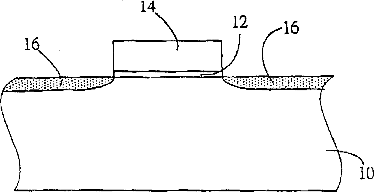
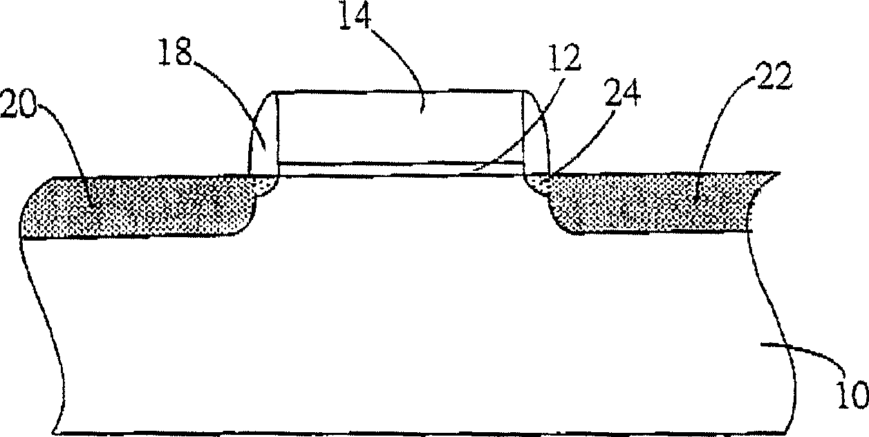
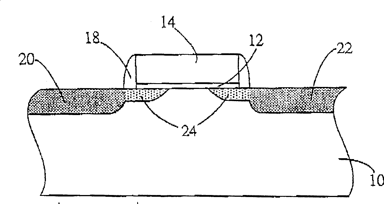
[0013] In the present invention, a gate stack structure is preformed on the substrate, and the gate stack structure is etched into a reverse trapezoidal shape, so that after the shallow ion doped region is formed, the shallow ion doped region is only laterally Diffusion to the substrate below the bottom edge of the gate stack structure, when heavy ion doping is performed to form an LDD structure, the length of the channel can be ensured, and the short channel effect commonly seen in sub-micron semiconductor manufacturing processes can be effectively solved.

[0014] Figure 2A to Figure 2E The schematic cross-sectional views of each step of making the LDD for a preferred embodiment of the present invention are respectively; as shown in the figure, the manufacturing method of the present invention includes the following steps:

[0015] see Figure 2A First, a gate oxide layer 22 is formed on the substrate 20; then a polysilicon layer 24 is deposited on the gate oxide layer 22,...


PUM


Abstract

In the method, a counter-trapeziodal structure with wide top edge and narrow bottom edge is formed by utilizing etching technique to etch grid stack structure after a gate oxide layer and grid stack structure of polysilicon layer are formed at the surface of a substrate. A vertical implanting step of shallow ion doping is carried on by utilizing the grid stack structure as shield to form a shallow ion doping region in the substrate at two sides of the grid stack stracture so the shallow ion doping region can be diffused horizontally to substrate under bottom periphery of the grid stack structure to form lightly doped drain structure in the following heat preparation process.

Description

【Technical field】 [0001] The present invention relates to a method for manufacturing a semiconductor device, in particular to a method for forming a lightly doped drain (LDD) by using a reverse trapezoidal gate structure to accurately control channel length. 【Background technique】 [0002] When the size of the semiconductor component is reduced, the channel length is also relatively reduced. At this time, the problem of short channel effect will occur. Known methods to solve the hot electron effect caused by the short channel effect are as follows: Figure 1A As shown, a gate stack structure of a gate oxide layer 12 and a polysilicon gate 14 is formed on the substrate 10 , and the polysilicon gate 14 is used as a shield to perform a shallow ion doping process to form a shallow ion doped region 16 . [0003] see next Figure 1B Form a spacer (spacer) 18 on both sides of the polysilicon gate 14, and use the spacer 18 and the polysilicon gate 14 as a shield to perform a deep do...

Claims


Application Information

Patent Timeline
Patent Type & Authority Applications(China)
IPC IPC(8): H01L21/28H01L21/336
Inventor 蔡孟锦金平中
Owner GRACE SEMICON MFG CORP
Why Eureka
Try Eureka