Fluted plane bigrid structure MOS device and its manufacturing method

A technology of MOS device and double gate structure, which can be used in semiconductor/solid-state device manufacturing, semiconductor devices, electrical components, etc., and can solve problems such as short channel effects

Inactive Publication Date: 2004-03-03
SEMICON MFG INT (SHANGHAI) CORP +1
View PDF0 Cites 9 Cited by
  • Summary
  • Abstract
  • Description
  • Claims
  • Application Information

AI Technical Summary

Problems solved by technology

However, many insurmountable difficulties are faced in the process of realizing sub-0.1 micron CMOS devices, such as: photolithography; p

Method used


Image

  • Fluted plane bigrid structure MOS device and its manufacturing method
  • Fluted plane bigrid structure MOS device and its manufacturing method
  • Fluted plane bigrid structure MOS device and its manufacturing method

Examples


Embodiment Construction

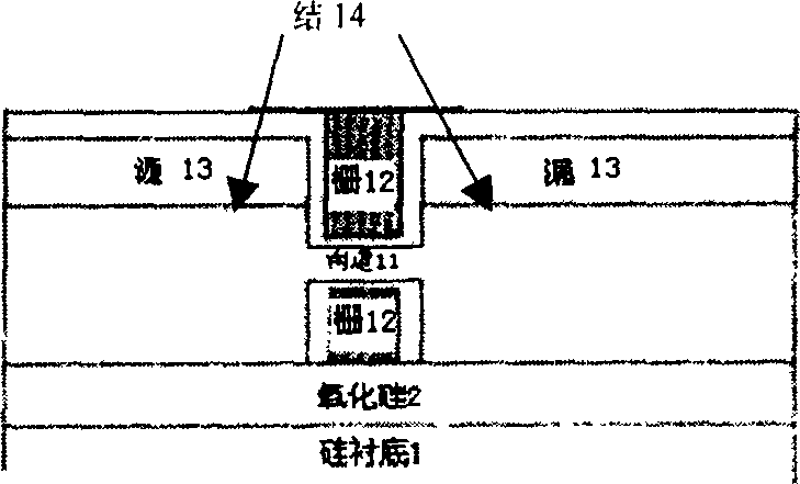
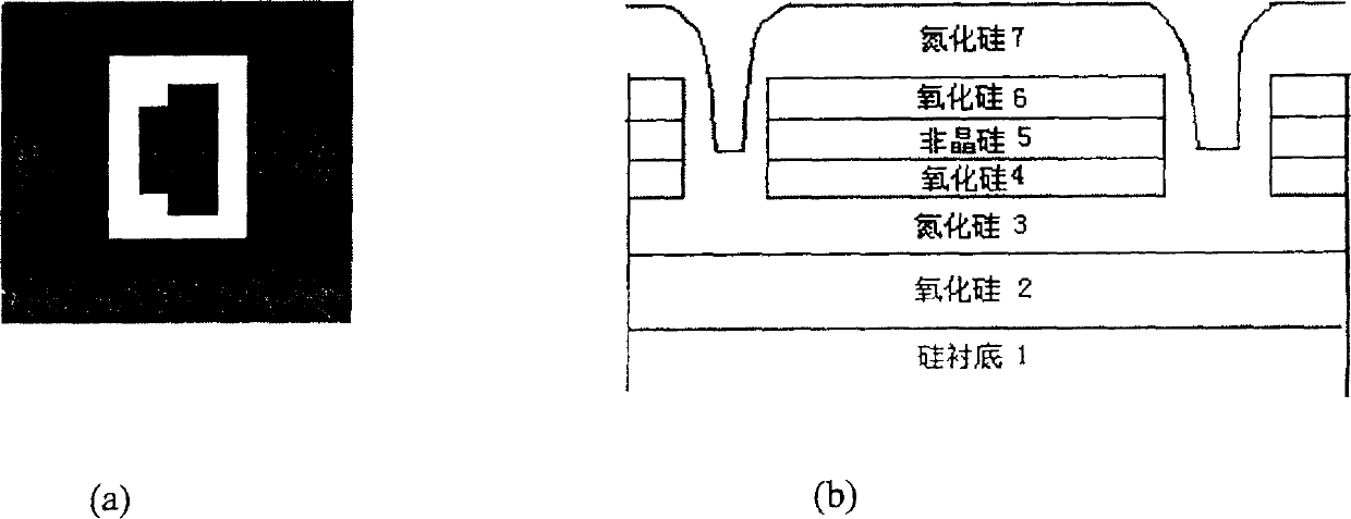
[0043] 1) To form the device structure as shown in Figure 1, first perform field oxidation on the single crystal silicon substrate 1 to form a buried oxide layer 2, and then deposit multiple layers of dielectrics, successively silicon nitride 3, silicon oxide 4, Amorphous silicon 5 and silicon oxide 6, as shown in Figure 2 (the first 9 steps in the process card).

[0044] 2) Lithograph the first layer (layout (a) in Figure 3, step 10 in the process card), etch off the top three layers to expose the silicon oxide layer 3 (steps 11-13 in the process card).

[0045] 3) As shown in Figure 3(b), deposit a layer of silicon nitride 7 to connect with the lower layer of silicon nitride 3 to ensure support for the hollowed out layer 8 (step 15 in the process card).

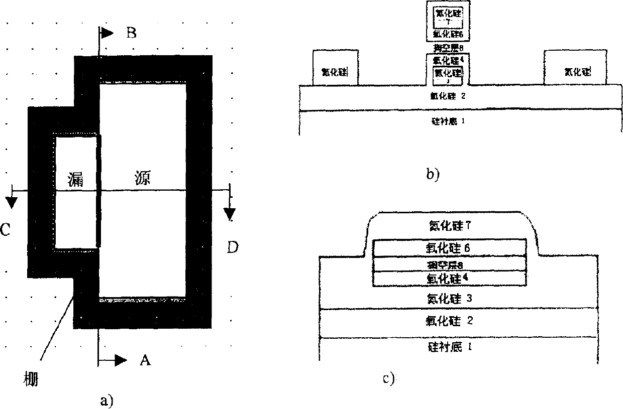
[0046] 4) Then perform the second photolithography (as shown in the layout (a) of Figure 4, step 22 in the process card), use electron beam exposure, and then etch (RIE) to etch dummy gate lines, from the top l...


PUM


Abstract

The part includes a substrate, a silicon monoxide layer. The silicon monoxide layer is deposited on the substrate, making entire part insulate from the substrate. Two grid electrodes are formed on silicon oxide layer. There is a groove between the two grid electrodes. The source electrode and drain electrode are formed on two sides of above grid electrode at plane higher than surface of the groove.

Description

technical field [0001] The invention belongs to the technical field of semiconductors, in particular to a novel grooved planar double-gate structure MOS (metal-oxide-semiconductor) device and a manufacturing method. Background technique [0002] Due to the reduction in circuit size, higher integration, faster speed and lower power consumption are required. In the past 25 years, planar MOS device technology has achieved great success in evolving from 5 μm to 0.13 μm in accordance with the principle of scaling down, and can smoothly develop to the 90nm node according to the roadmap (Roadmap) of the International Semiconductor Association (SIA) in 2001. However, many insurmountable difficulties are faced in the process of realizing sub-0.1 micron CMOS devices, such as: photolithography; power supply voltage and threshold voltage; short channel effect; gate oxide layer; high field effect; random distribution of doping curve . In order to break through these limitations, innova...

Claims


Application Information

Patent Timeline
IPC IPC(8): H01L21/336H01L29/78
Inventor 卓铭徐秋霞
Owner SEMICON MFG INT (SHANGHAI) CORP
Why Eureka
Try Eureka