Method for forming self-alignment metal silicide

A metal silicide, metal layer technology, applied in electrical components, semiconductor/solid-state device manufacturing, circuits, etc., to solve problems such as short circuits, conductive impurities, and component failures

Inactive Publication Date: 2004-03-24
GRACE SEMICON MFG CORP
View PDF0 Cites 15 Cited by
  • Summary
  • Abstract
  • Description
  • Claims
  • Application Information

AI Technical Summary

Problems solved by technology

However, in the above-mentioned conventional process, the silicon atoms in the gate structure or the source/drain region will diffuse to the gate spacer to form titanium silicide (TiSi 2 ) metal silicide, or oxygen atoms diffuse through the titanium metal layer to the sidewall of the gate spacer due to high temperature to form conductive titanium oxide, or the temperature of the self-aligned metal silicide reaction (salicidation) is improper. Various other reasons for the reaction of silicon dioxide to produce titanium silicide, etc.; due to these fac

Method used


Image

  • Method for forming self-alignment metal silicide
  • Method for forming self-alignment metal silicide
  • Method for forming self-alignment metal silicide

Examples


Embodiment Construction

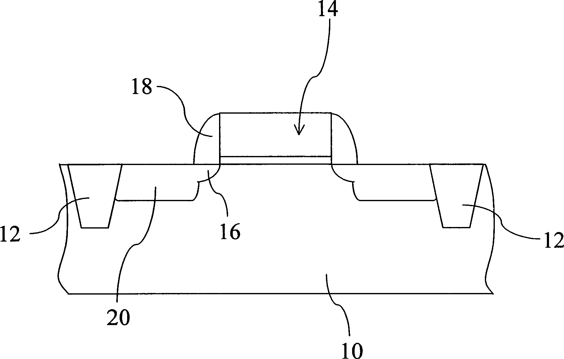
[0012] In the conventional manufacturing process of self-aligned metal silicide, it is very easy to cause conductive non-deposits on the sidewall of the gate spacer between the gate structure and the source / drain region, which will cause a short circuit. lead to component failure, and the method proposed by the present invention can effectively overcome these deficiencies in the prior art.

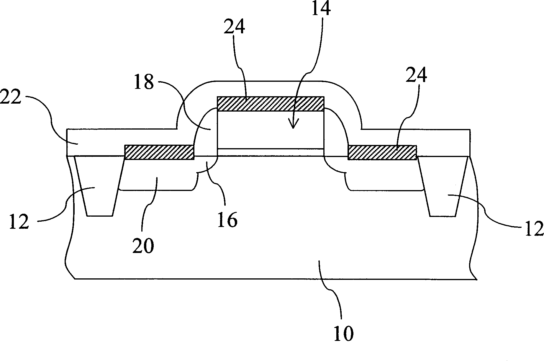
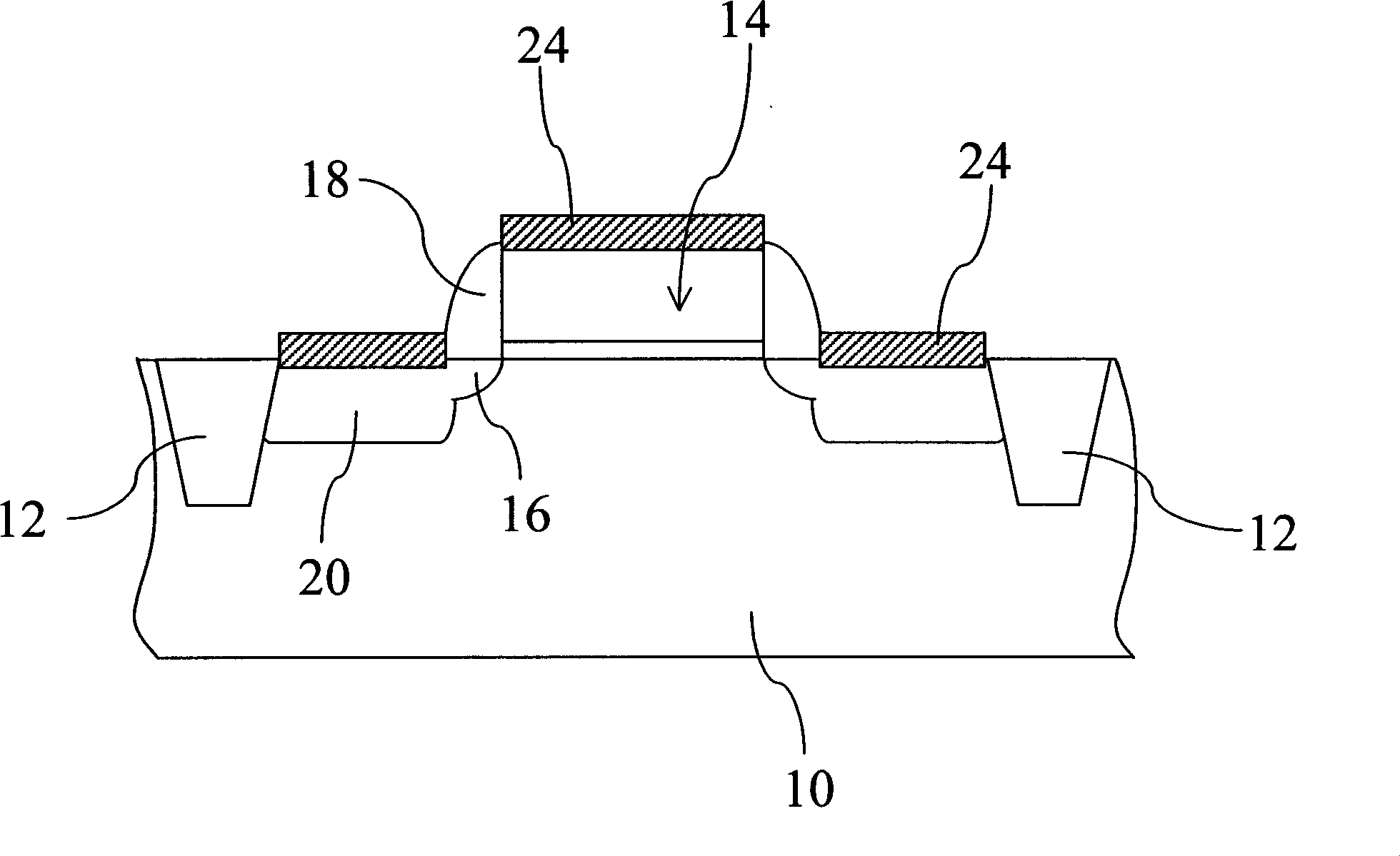
[0013] 2( a ) to FIG. 2( d ) are cross-sectional views of each step in the fabrication of self-aligned metal silicide in a preferred embodiment of the present invention. First, as shown in FIG. 2( a), a shallow trench isolation region (shallow trench isolation, STI) 32 is first formed in a semiconductor substrate 30 to isolate active components and passive components in the semiconductor substrate 30; A transistor gate structure 34 is formed on the surface of the substrate 30, which is composed of a gate oxide layer 342 and a polysilicon layer 344 thereon; and then the semiconductor substr...


PUM


Abstract

This invention provides a method for forming a self-aligning metal silicide which forms an isolation zone, transistor grating structure and a light doped source/drain zone on a semiconductor base, and a grating gap wall on the grating side wall containing a silicon oxide layer and a silicon nitride layer on it then a heavy doped source/drain zone, and to form a blocking layer on the metal layer before forming metal silicide by heat annealing in the successive process of self-aligning metal silicide, utilizing the silicon nitride layer of the said grating gap wall and the said blocking layer to stop Si atoms and O actoms from diffusing to the side wall of the grating gap wall to avoid short circuit.

Description

technical field [0001] The present invention relates to a method for forming a self-aligned silicide (Self-aligned Silicide, SALICIDE), in particular to a method for forming a self-aligned silicide that can avoid short circuits caused by gate spacers method. Background technique [0002] When the production of semiconductor components enters the deep sub-micron process, and the integration of integrated circuits is getting higher and higher, the size of the components is getting smaller and smaller, so that the area of ​​the gate and source / drain regions is also reduced, and in order to reduce The serial resistance of components, the reduction of the number of metal contact windows, and the convenience of subsequent connection wire layout (Layout) are increased, thereby reducing the entire component arrangement area. The use of automatic alignment metal silicide technology has gradually been widely used in semiconductor manufacturing processes. [0003] In the deep sub-micr...

Claims


Application Information

Patent Timeline
IPC IPC(8): H01L21/285H01L21/311H01L21/3205H01L21/3213H01L21/336
Inventor 高荣正
Owner GRACE SEMICON MFG CORP
Why Eureka
Try Eureka