Magnetic RAM, its mfg. and driving method

A technology of random access memory and magnetic tunnel junction, which is applied in static memory, digital memory information, semiconductor/solid state device manufacturing, etc.

Inactive Publication Date: 2004-05-26
SAMSUNG ELECTRONICS CO LTD
View PDF0 Cites 6 Cited by
  • Summary
  • Abstract
  • Description
  • Claims
  • Application Information

AI Technical Summary

Problems solved by technology

Therefore, when the magnetoresistance (MR) rate of the MTJ layer is low, data recorded in the MTJ layer cannot be accurately read out, and the use of MRAM is limited.

Method used


Image

  • Magnetic RAM, its mfg. and driving method
  • Magnetic RAM, its mfg. and driving method
  • Magnetic RAM, its mfg. and driving method

Examples


Embodiment Construction

[0027] An MRAM according to an embodiment of the present invention and methods of manufacturing and driving the same will be described in detail with reference to the accompanying drawings. In the drawings, the shapes of elements are exaggerated for clarity.

[0028] First, the MRAM according to the present invention will be explained.

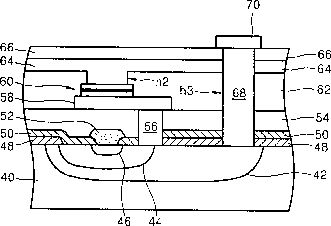
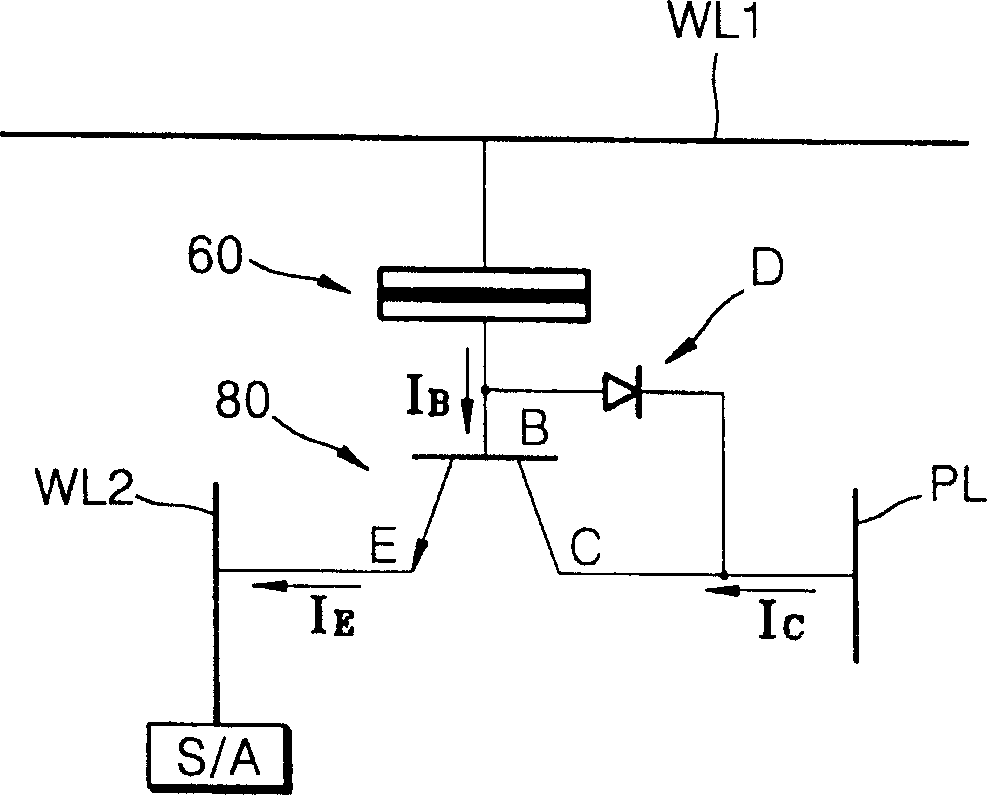
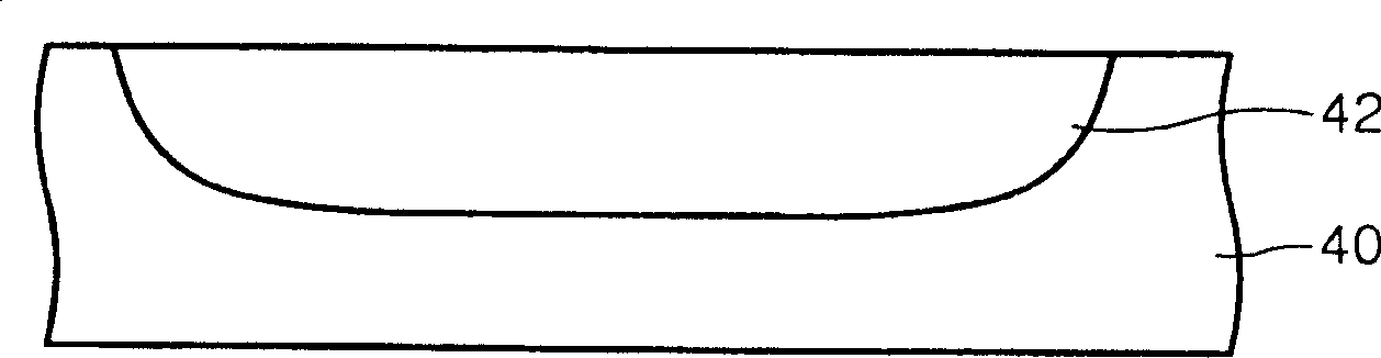
[0029] see figure 1 , the n-type first impurity region 42 is formed by doping a first conductive impurity such as phosphorus (P) in the semiconductor substrate 40 to a predetermined depth. The n-type first impurity region 42 functions as a collector of a bipolar junction transistor (BJT). The p-type impurity region 44 is formed by doping second conductive impurities such as boron (B) in the n-type first impurity region 42 . The p-type impurity region 44 serves as the base of the BJT. no + The p-type second impurity region 46 is formed by doping the p-type impurity region 44 with third conductive impurities. no + Type second impurity reg...


PUM


Abstract

Provided are an MRAM and methods for manufacturing and driving the same. The MRAM includes a bit line coupled to an emitter of a bipolar junction transistor (BJT), a magnetic tunneling junction (MTJ) layer coupled to the BJT, a word line coupled to the MTJ layer, a plate line coupled to the BJT so as to be spaced apart from the MTJ layer, and an interlayer dielectric formed between the components. The MTJ layer is coupled to a base and a collector of the BJT, the plate line is coupled to the collector, and an amplifying unit for amplifying a data signal during a read operation of data stored in the MTJ layer is coupled to the bit line. Because the bit line is formed of a metal and the BJT is used, a series resistance effect caused by the resistance of a MOS transistor and the parasitic resistances of other elements can be minimized, thus allowing data to be precisely read out from the MTJ layer. Also, compared to an MRAM with a MOS transistor, the MRAM with the BJT leads to improved integration density and can use an MTJ layer having a low MR ratio.

Description

technical field [0001] The present invention relates to a semiconductor memory and its manufacturing and driving method, in particular to a magnetic RAM (MRAM) and its manufacturing and driving method. Background technique [0002] MRAM (Magnetic Random Access Memory), one of next-generation memories, has the performance of both DRAM and SRAM, and also has the non-volatility of flash memory. [0003] In general, an MRAM includes MOS transistors connected to each other and a magnetic tunnel junction (MTJ) layer in which data is stored. In this MRAM, the resistance of the MOS transistors limits the choice of the MTJ layer. In addition, the tunnel current flowing through the MTJ layer flows through the MOS transistor. Therefore, when the magnetoresistance (MR) rate of the MTJ layer is low, data recorded in the MTJ layer cannot be accurately read, and the use of the MRAM is limited. Contents of the invention [0004] The present invention provides an MRAM that can increase ...

Claims


Application Information

Patent Timeline
Patent Type & Authority Applications(China)
IPC IPC(8): H01L27/105G11C11/00G11C11/15G11C11/16H01L21/8246H01L27/102H01L27/22H01L43/08
CPCG11C11/16B82Y10/00H01L27/226H10B61/20G11C11/15
Inventor 柳寅儆朴玩浚
Owner SAMSUNG ELECTRONICS CO LTD
Why Eureka
Try Eureka