Delay locking loop having acceleration mode and controlled by register

A technology of delay-locked loop and acceleration mode, which is applied in the direction of automatic power control, static memory, digital memory information, etc., and can solve the problems of reducing accuracy and complex execution

Inactive Publication Date: 2004-05-26
SK HYNIX INC
View PDF0 Cites 15 Cited by
  • Summary
  • Abstract
  • Description
  • Claims
  • Application Information

AI Technical Summary

Problems solved by technology

[0022] However, in the prior art, there is such a problem that not only the input clock signal rclk without delay is provided to the input clock signal of the first phase comparator 40 and the second phase comparator 44, but also the input clock signal rclk without delay is divided. With a reference clock signal ref of 1 / M
[0023] Although, in this example, it is easy to control the semiconductor memory device and reduce current consumption by using a divided clock signal such as the reference clock signal ref, various necessary timing specifications are required as the execution speed of the memory device increases. , which reduces the accuracy of the execution and becomes more complex

Method used


Image

  • Delay locking loop having acceleration mode and controlled by register
  • Delay locking loop having acceleration mode and controlled by register
  • Delay locking loop having acceleration mode and controlled by register

Examples


Embodiment Construction

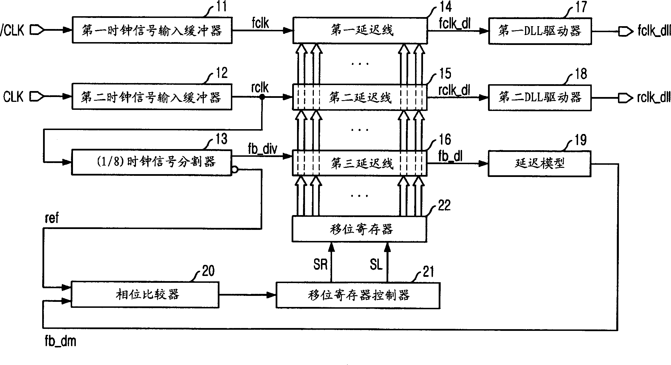
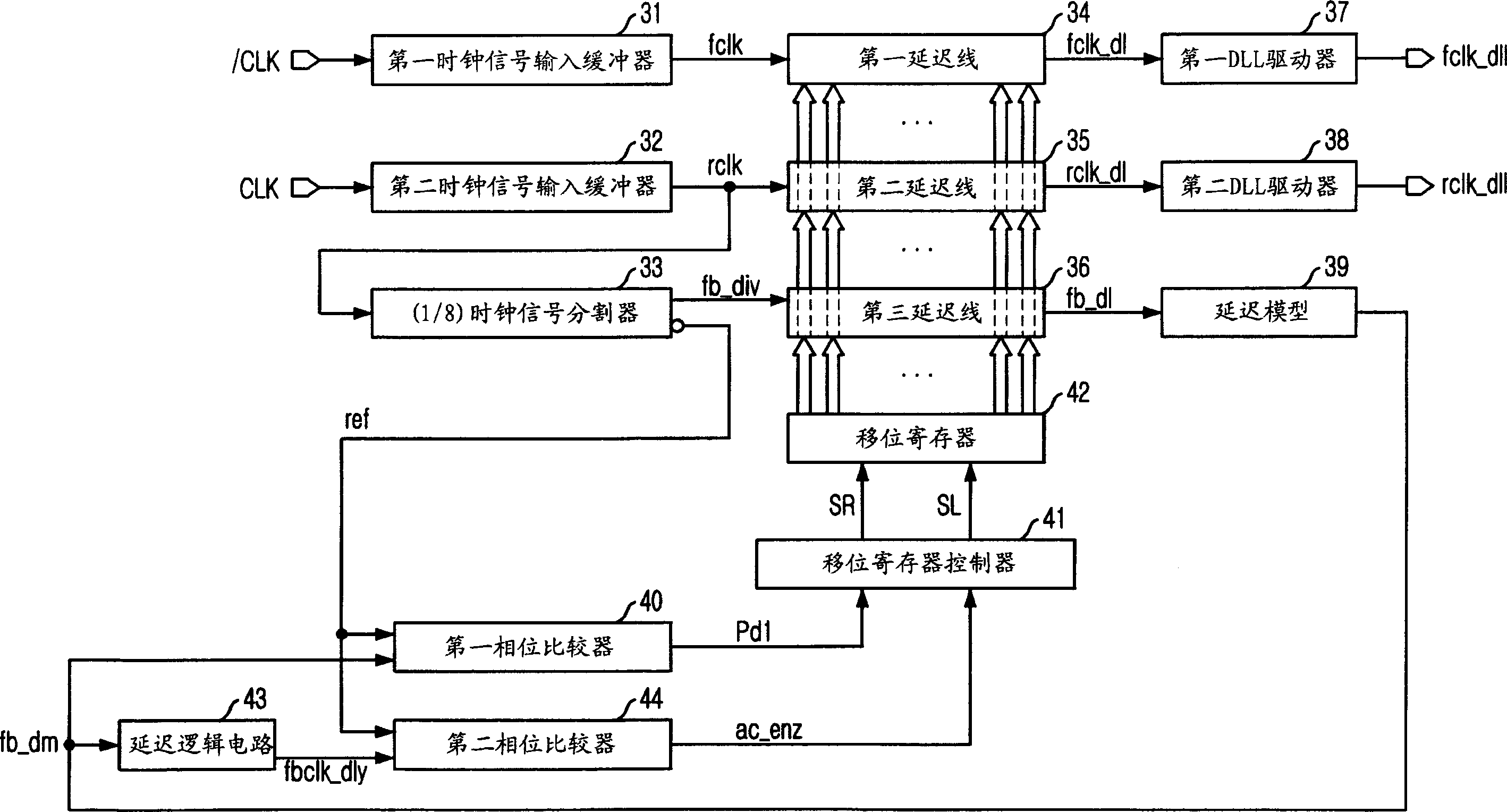
[0036] The present invention relates to a method for controlling an acceleration mode using a technique that does not use two clock signals supplied to a phase comparator and compares them with each other by using the phase comparator.

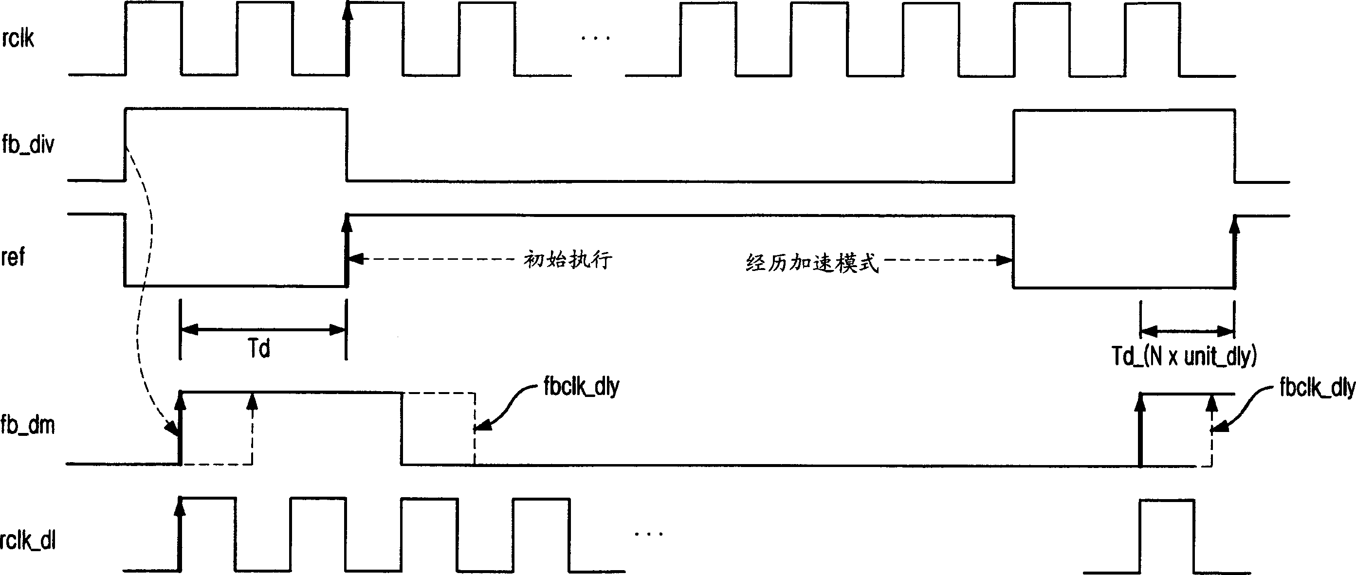
[0037] The present invention uses an input clock signal without delay as the clock signal source. A first phase comparator compares the undelayed input clock signal to the output from the delay model, and a second phase comparator compares the undelayed input clock signal to the clock signal output from the delay logic circuit. The outputs of the first and second phase comparators determine whether the overdrive mode is implemented on the mode decision logic. What is important is that by doing this in the speedup mode, N delay element units jump and shift in the shift register immediately, and the shifted delay value must be the same as the delay value N×unit_delay of the delay logic circuit.

[0038] Hereinafter, a semiconductor memory devic...


PUM


Abstract

The present invention provides for a register controlled delay locked loop having an acceleration mode for improving accuracy to be correspondent to an increase of the operation speed of a memory device. For this object, in the present intention, the register controlled delay locked loop includes a delay line, a delay model, a delay means, a first and a second phase comparators, a mode decision means, a shift register control means, and a shift register.

Description

technical field [0001] The present invention relates to a semiconductor circuit technology, and more particularly, to a register-controlled delay-locked loop (DLL) with a boost mode. Background technique [0002] In general, a clock signal of a system or a circuit is used as a reference quantity for synchronously performing timing and ensuring error-free high-speed operation. When an external clock signal of an external circuit is used in an internal circuit, a clock signal skew is generated from the internal circuit due to a timing gap between the external clock signal and the internal clock signal. A delay locked loop (hereinafter referred to as DLL) compensates clock signal skew so that the phase of the internal clock signal is equal to the phase of the external clock signal. [0003] In addition, DLLs are widely used in synchronous semiconductors including Double Data Rate Synchronous Dynamic Random Access Memory (DDR SDRAM) due to their advantage of being less suscepti...

Claims


Application Information

Patent Timeline
Patent Type & Authority Applications(China)
IPC IPC(8): G06F1/12G11C11/407G11C11/4076H03K5/131H03K5/135H03L7/081H03L7/087H03L7/107
CPCH03L7/107H03L7/0814H03L7/0805H03L7/087H03L7/0816
Inventor 郭钟太李星勋
Owner SK HYNIX INC
Why Eureka
Try Eureka