Nonvolatile memory cell and non-volatile semiconductor memory device

A non-volatile storage and storage unit technology, applied in semiconductor devices, semiconductor/solid-state device manufacturing, information storage, etc., can solve the problems that the bit line current difference cannot be increased, the manufacturing cost is greatly affected, and the storage array area is increased.

Active Publication Date: 2004-06-16
SAMSUNG ELECTRONICS CO LTD
View PDF2 Cites 32 Cited by
  • Summary
  • Abstract
  • Description
  • Claims
  • Application Information

AI Technical Summary

Problems solved by technology

In order to improve the driving capability of the selection transistor 3, although the above-mentioned method of increasing the gate width of the transistor is effective, the transistors are connected to each RRAM element 2, and there are many transistors, so increasing the gate width will cause The overall area of ​​the storage array increases, which greatly affects the manufacturing cost
As a conclusion, the on-resistance of the select transistor 3 becomes a large factor that the above-mentioned bit line current difference cannot increase

Method used


Image

  • Nonvolatile memory cell and non-volatile semiconductor memory device
  • Nonvolatile memory cell and non-volatile semiconductor memory device
  • Nonvolatile memory cell and non-volatile semiconductor memory device

Examples


no. 1 Embodiment approach

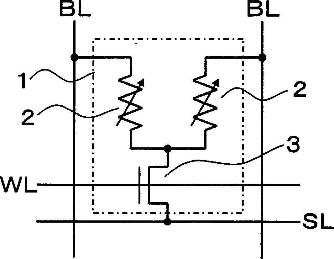
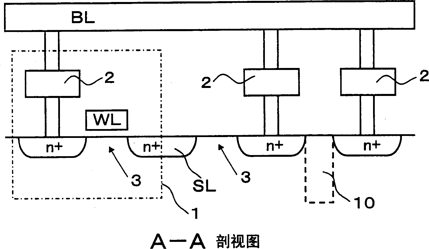
[0047] figure 1 The structure of the storage unit 1 of the apparatus of the present invention is shown in . The memory cell 1 is equipped with: two variable resistance elements; and a selection transistor 3 constituted with one N-type MOSFET as a selection element for selecting the two variable resistance elements, and one end of each variable resistance element 2 is connected to the end of the selection transistor 3 respectively. Drain connection. In addition, the other end of each variable resistance element 2 is connected to a different bit line BL, the gate of the selection transistor 3 is connected to the word line WL, and the source of the selection transistor 3 is connected to the source line SL. In this embodiment, since two variable resistance elements 2 are provided in one memory cell, the same Figure 17 Compared with the conventional memory cell shown, although it has twice the storage capacity, if one variable resistance element 2 corresponds to one memory cell...

no. 2 Embodiment approach

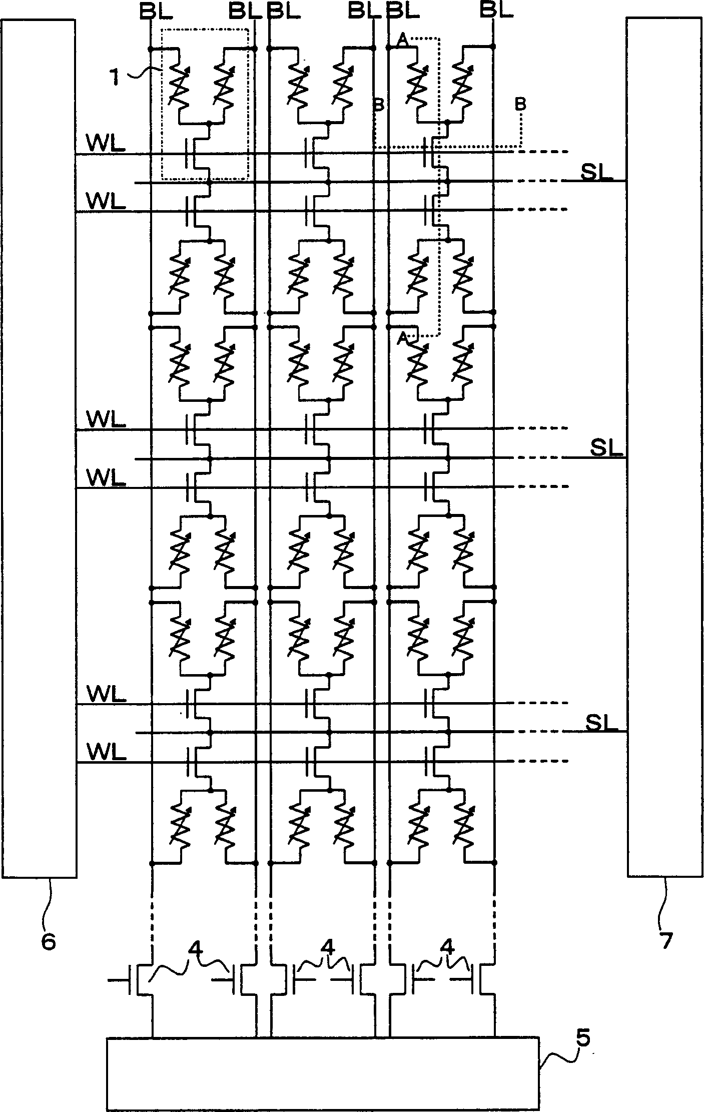
[0052] Then, respectively, in Figure 4 Indicates that a memory array with a layered bit line structure is used on the substrate. Figure 5 An example of a readout circuit in this layered bit line structure is shown in . In order to realize high-speed and stable reading of stored data from memory cell 1, it can be made as Figure 4 The memory array structure of the hierarchical bit line structure is shown.

[0053] In the hierarchical bit line structure of this embodiment, the bit line directly connected to the memory cell 1 is called a local bit line LBL. A memory array connected to the same local bit line LBL in the column direction is regarded as one block, a plurality of blocks are arranged in the column direction, and a local bit line selection transistor 11 for selecting the local bit line LBL of each block is provided, and the local bit line LBL passes through the local bit line. Bit line selection transistor 11 is connected to global bit line GBL. In addition, the ...

no. 3 Embodiment approach

[0058] Figure 7 A third embodiment of the device of the present invention is shown. and Figure 4 The difference in the second embodiment shown is that a pair of local bit lines LBL1 and LBL2 connected to the same memory cell 1 is connected to equalize the pair of local bit lines LBL1 and LBL2 to the same potential during the charging period. Transistor 13 is used. Such as Figure 8 As shown in the signal timing waveform diagram, in the second embodiment, although the bit line selection signal BK2 is temporarily at a high level during the charging period, in the third embodiment, the local bit line selection signal BK2 is maintained at a low level , On the other hand, the equalization signal EQ1 is at a high level during the charging period, so that the equalization transistor 13 is turned on, and the local bit line LBL2 is charged. Only the method of charging a pair of local bit lines LBL1 and LBL2 is different, and other operations are the same as those of the second em...


PUM


Abstract

It is an object of the present invention to make it possible to decrease the on-state resistance of a selection transistor of a memory cell without increasing the whole area of a memory cell array and accelerate and stabilize the reading operation of data stored in the memory cell. Therefore, a plurality of variable resistive elements capable of storing information in accordance with a change of electrical resistances is included, one ends of the variable resistive elements are connected each other, and an electrode of a selection element constituted by a MOSFET or diode element for selecting the variable resistive elements in common is connected with one end of each of the variable resistive elements to constitute a memory cell.

Description

technical field [0001] The present invention relates to a nonvolatile semiconductor memory device and a memory cell used therein, and more particularly to a nonvolatile semiconductor memory device in which the memory cell has a variable resistance element capable of storing information by utilizing a change in resistance. Background technique [0002] At present, there are MRAM (Magnetic RAM), OUM (Ovonic Unified Memory), RRAM (Resistance control nonvolatile Random Access Memory), etc. . These elements store information by changing resistance, and realize a nonvolatile memory device by reading information by changing the resistance value. For example, MRAM uses MTJ (Magnetic Tunnel Junction) elements to form a memory cell, and its content is disclosed in Japanese Unexamined Patent Publication No. 2002-151661, for example. Figure 16 The middle indicates the partial configuration related to the readout of the memory cell configuration. In addition, as a memory cell using an...

Claims


Application Information

Patent Timeline
Patent Type & Authority Applications(China)
IPC IPC(8): G11C11/15G11C11/16G11C13/00H01L21/8246H01L27/10H01L27/105H01L27/24H01L43/08
CPCG11C11/16G11C11/5685G11C2213/78G11C2213/79G11C2213/31G11C2213/72G11C13/0007G11C13/003G11C11/15H01L27/24H10B63/20H10B63/30H10B63/80H10N70/20H10N70/8836H10N70/826H10B63/00
Inventor 森川佳直
Owner SAMSUNG ELECTRONICS CO LTD
Why Eureka
Try Eureka