Method for forming image on object surface including circuit substrate

A technology for circuit substrates and multilayer circuit substrates, applied to the removal of conductive materials by discharge methods, printed circuits, and printed circuit manufacturing, which can solve unavoidable problems

Inactive Publication Date: 2004-08-11
DAIKEN CHEM
View PDF0 Cites 9 Cited by
  • Summary
  • Abstract
  • Description
  • Claims
  • Application Information

AI Technical Summary

Problems solved by technology

However, due to restrictions on the use of photomasks, the same disadvantages as circuit boards are inevitable in terms of image patterns.

Method used


Image

  • Method for forming image on object surface including circuit substrate
  • Method for forming image on object surface including circuit substrate
  • Method for forming image on object surface including circuit substrate

Examples


Embodiment Construction

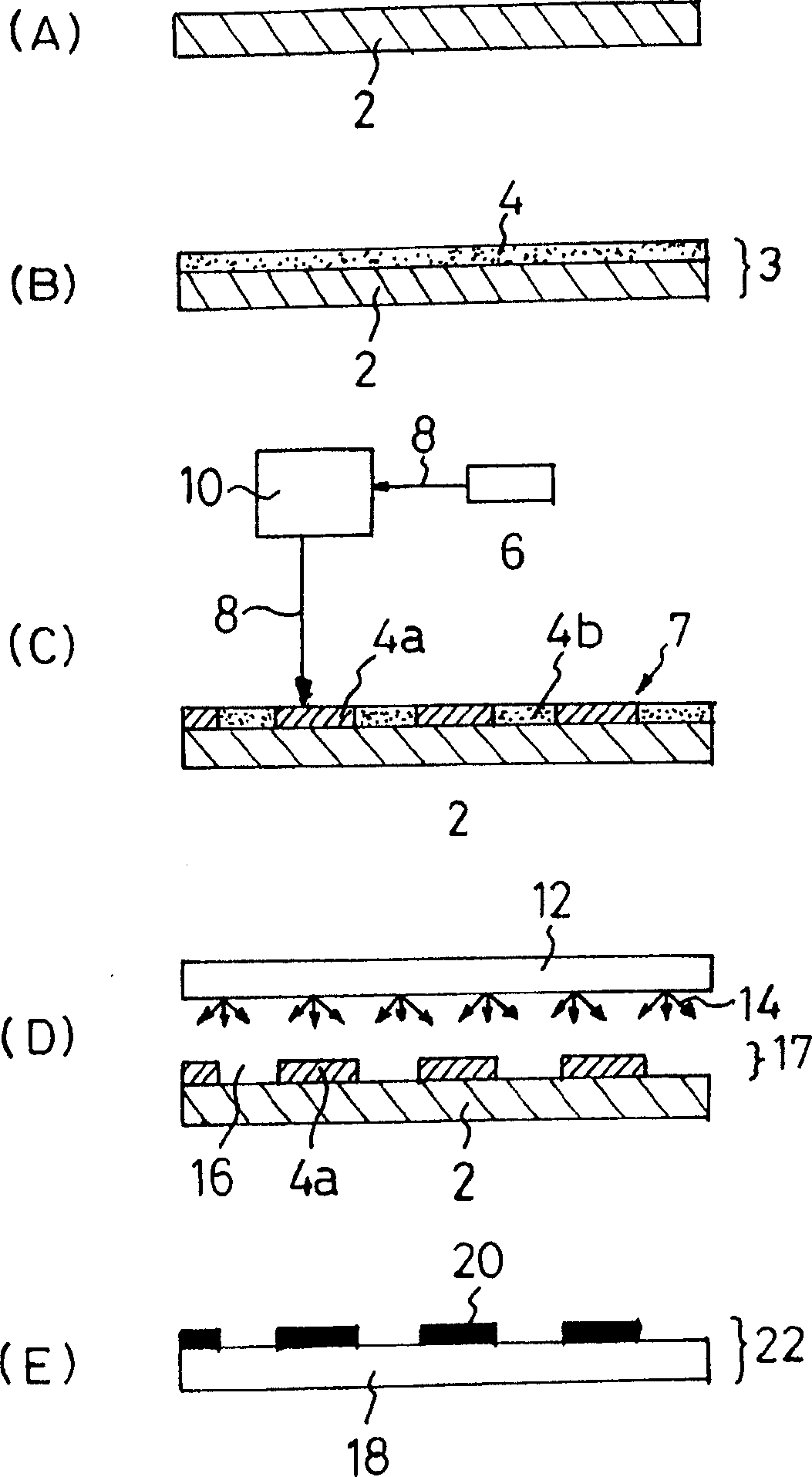
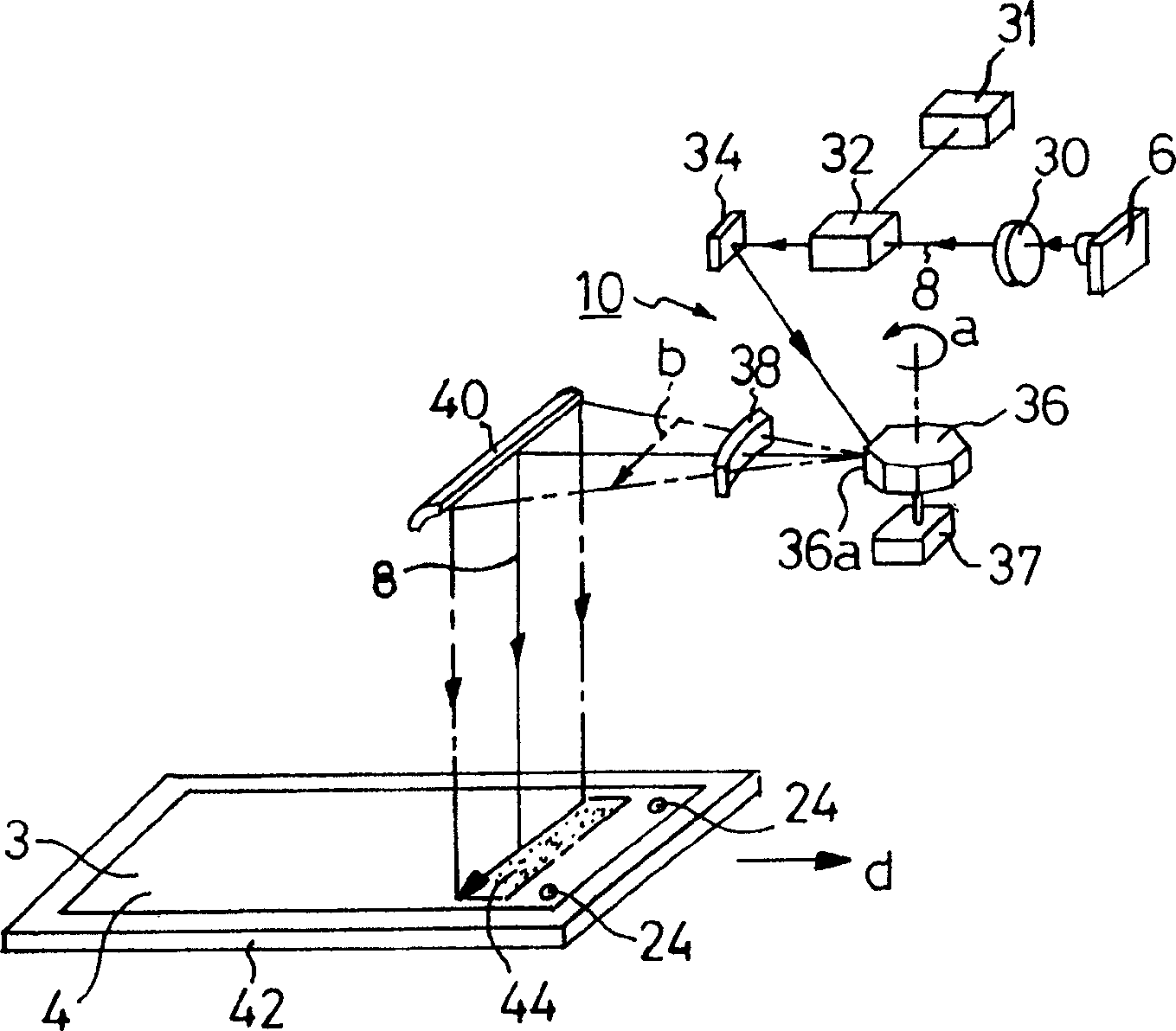
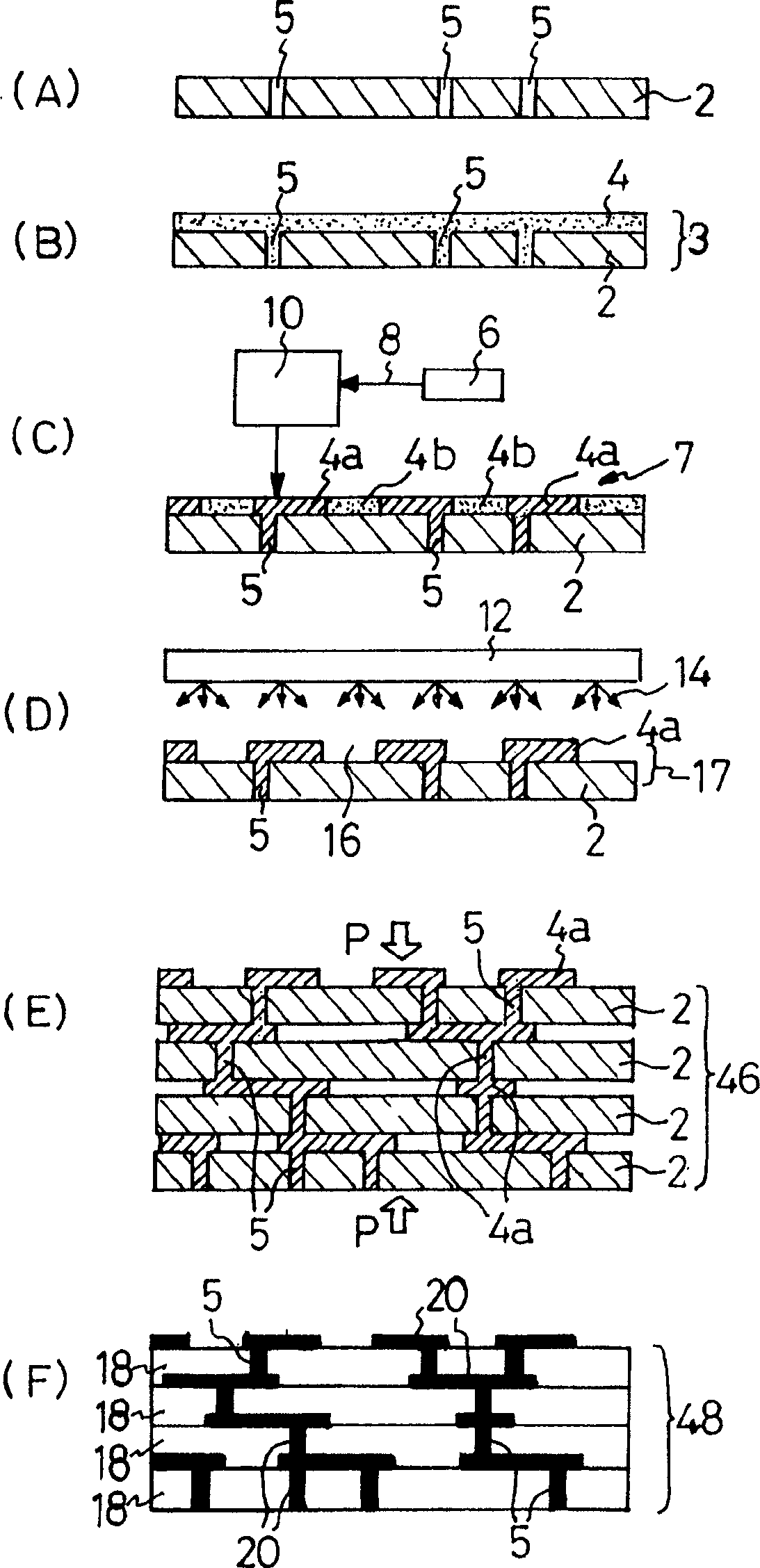
[0042] Hereinafter, embodiments of the circuit board manufacturing method of the present invention will be described in detail with reference to the drawings.

[0043] figure 1 It is a manufacturing process diagram of the single-layer type circuit board as the first embodiment of the present invention. In the step (A), the green sheet 2 to be a circuit board is placed at a predetermined position. First, adjust the ceramic powder that will become the raw material sheet 2 preparation. As for the ceramic powder, various materials can be used. For example, mix CaO·Al at a weight ratio of 60:40 2 o 3 ·B 2 o 3 ·SiO2 2 A mixture of borosilicate glass powder and alumina powder is also acceptable.

[0044] Form the ceramic powder into a paste with an organic solvent, an organic binder, and a plasticizer. For example, use a doctor blade method to form the paste into a sheet with a thickness of 1-300 μm, and roll it up to form a raw material tape. This raw material tape is cut ...


PUM


Abstract

By using a novel method, the exposure time of the photosensitive paste layer is reduced and the exposure fineness of the layer is improved, thereby developing a highly fine circuit substrate of high density having a thermal resistance at a reasonable cost. A circuit substrate is manufactured as follows. A photosensitive paste containing photoresist and a circuit material is applied onto a substrate surface so as to form a photosensitive paste layer (4). This photosensitive paste layer (4) is plotted by a laser beam (8) so as to form a plotted area (7). The photosensitive paste layer (4) is developed and an exposed area (4a) or an unexposed area (4b) is removed so as to form a circuit pattern (17). This circuit pattern (17) is sintered to form a circuit pattern (20) composed of the circuit material. It is possible to form a highly fine circuit pattern of high density by laser beam plotting. Moreover, when a greensheet (2) is used as the substrate, it is possible to form a ceramic substrate (18) having a thermal resistance by sintering. Furthermore, by using this method, it is possible to form an arbitrary image on an arbitrary object.

Description

technical field [0001] The present invention relates to the method for forming image graphics on the surface of substrates and the like, and in more detail, relates to the photosensitive adhesive layer formed by mixing coloring materials and photoresists, scanning and irradiating laser beams to form an extremely high The drawing area composed of fine image graphics develops the photosensitive adhesive layer to form an image forming method of high-definition image graphics on the surface of the object. Background technique [0002] As objects on which image patterns are formed, there are circuit boards, magcups, crafts, and the like. The circuit substrate is an object that forms a circuit pattern on the surface of the substrate, the porcelain bottle is an object that forms a decorative image on the outer peripheral surface of a cylinder made of ceramics, and most of the handicrafts are objects that form a process decorative image on the surface of a craft item. Among these o...

Claims


Application Information

Patent Timeline
Patent Type & Authority Applications(China)
IPC IPC(8): H05K1/09H05K3/02H05K3/46
CPCH05K3/02H05K1/092H05K2203/0514Y10S430/146H05K3/4611H05K2203/107H05K3/08
Inventor 加藤正利原田昭雄
Owner DAIKEN CHEM
Why Eureka
Try Eureka