Defect detector, defect detecting method and method for detecting hole figure

A defect inspection and defect technology, applied in the direction of measuring devices, optical devices, instruments, etc., can solve problems such as noise formation, insufficient inspection, and deterioration of S/N ratio

Active Publication Date: 2004-09-29
NIKON CORP
View PDF0 Cites 29 Cited by
  • Summary
  • Abstract
  • Description
  • Claims
  • Application Information

AI Technical Summary

Problems solved by technology

Therefore, when the influence of the base pattern is large, noise will be formed, and the pattern information of the uppermost layer that should be inspected will be relatively reduced, thereby deteriorating the S/N ratio.
In particular, since the hole patterns

Method used


Image

  • Defect detector, defect detecting method and method for detecting hole figure
  • Defect detector, defect detecting method and method for detecting hole figure
  • Defect detector, defect detecting method and method for detecting hole figure

Examples


Embodiment Construction

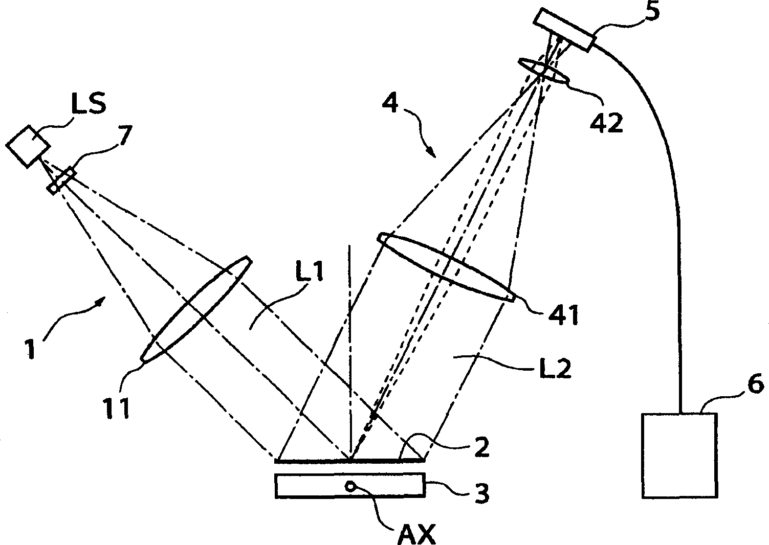
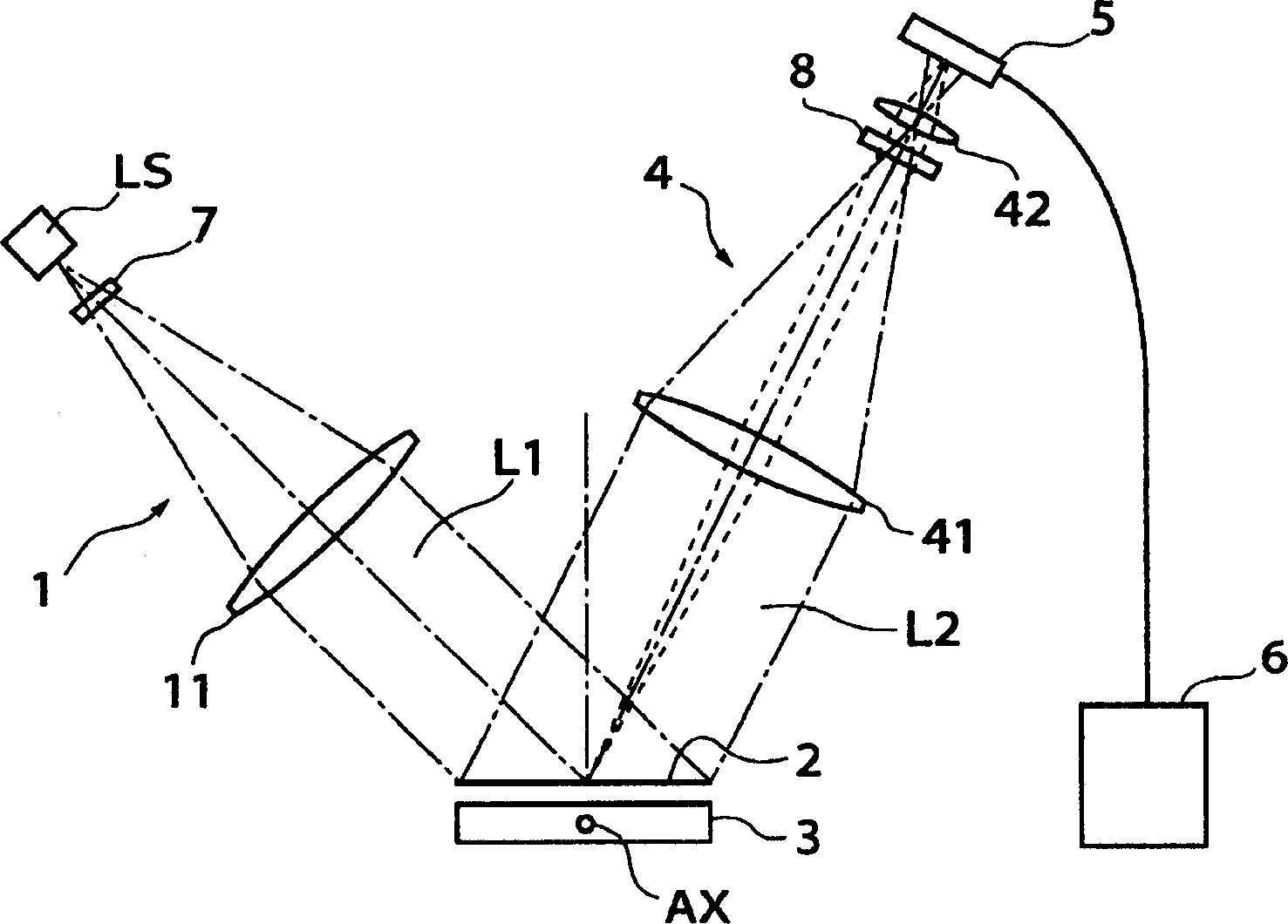
[0037] Examples of embodiments of the present invention will be described below using the drawings. figure 1 It is a schematic diagram of the defect inspection device according to the first embodiment of the present invention. The illumination light L1 emitted from the light source LS (lamphouse) is converted into substantially parallel light by the lens 11 constituting the illumination optical system 1 , and illuminates the wafer 2 placed on the stage 3 . A light source such as a halogen lamp or a metal halide lamp (not shown) and a wavelength selection filter are incorporated in the light source LS, and only light of a part of wavelength is used as illumination light L1.

[0038] The polarizing plate 7 is arranged in the vicinity of the emitting portion of the light source LS to make the illumination light L1 emitted from the light source LS linearly polarized. The polarizing plate 7 can rotate around the optical axis of the illumination optical system 1 to arbitrarily cha...


PUM


Abstract

Provided is a device for inspecting defects, which can inspect a pattern of a top layer with a high S/N ratio. In the device, diffracted light L2 produced by a wafer 2 being a substrate which is illuminated by illumination light L1 is guided and collected by a light receiving optical system 4 composed of a lens 41 and a lens 42, and the diffracted light L2 forming an image of the wafer 2 is focused on an image pickup device 5 used as an imaging means. The image acquired by the image pickup device 5 is subjected to an image processing step carried out by an image processing device 6, thereby detecting the defect. A polarizer 7 is adjusted so that the illumination light L1 illuminates the wafer 2 in S polarization. Because the S polarization makes a surface reflectivity higher, the amount of light reaching a base portion is reduced. Accordingly, the amount of light reflected by the top layer can be made larger than that reflected by the base portion, by using the S polarization for the illumination, thereby enabling the defect of the top layer to be inspected with the high S/N ratio.

Description

technical field [0001] The present invention relates to a defect inspection device and defect inspection method for inspecting defects such as unevenness and damage on the surface of a substrate, and a method for inspecting hole patterns such as contact holes, for example, in a manufacturing process of a semiconductor element or the like. Background technique [0002] In the manufacture of semiconductor devices and liquid crystal substrates, the work of forming various circuit patterns and stacking them in several layers is repeated. The outline of the process of forming each circuit pattern is to apply a photoresist on the surface of the substrate, use an exposure device to burn out the circuit pattern on the photoresist and the index line and the mask, and form a photoresist through development. After the circuit pattern formed by the resist, each part of the element is formed by etching or the like. After forming a pattern of photoresist, the pattern is checked for abnor...

Claims


Application Information

Patent Timeline
IPC IPC(8): G01B11/30G01N21/956H01L21/66
CPCG01N21/95692G01N21/956G01B11/30
Inventor 杉原麻理大森健雄深泽和彦
Owner NIKON CORP
Why Eureka
Try Eureka