
Film optical addressing electric potential sensor used for detecting Hg2+ and preparation method thereof
A potential sensor and optical addressing technology, which is applied in the direction of instruments, measuring devices, scientific instruments, etc., can solve the problems of complex preprocessing, long measurement cycle, and huge equipment, and achieve less sample solution, fast measurement, and convenient use Effect
- Summary
- Abstract
- Description
- Claims
- Application Information
AI Technical Summary
Problems solved by technology
Method used
Image

Examples
Embodiment Construction
[0023] Structure of the sensor
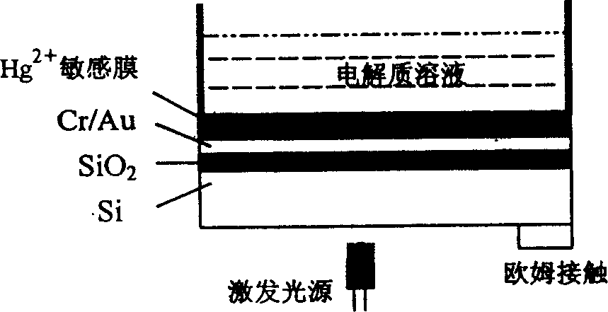
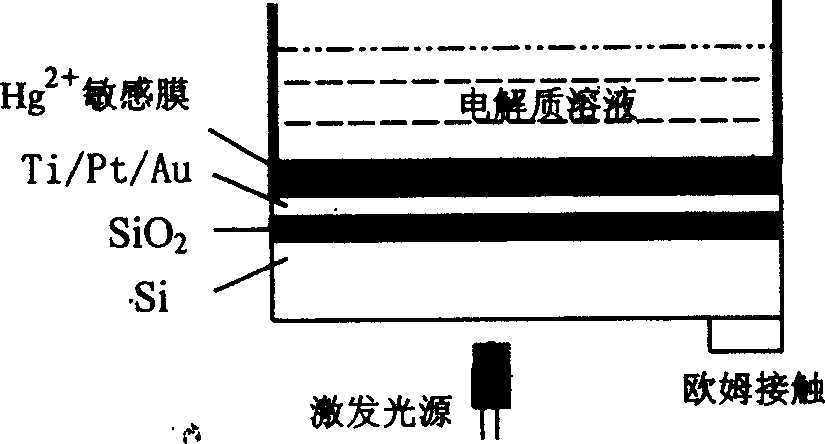
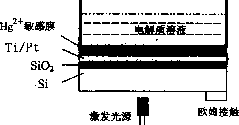
[0024] Use p-type or n-type Si sheets as the substrate, and there are SiO on the substrate from bottom to top. 2 layer, metal layer, for Hg 2+ sensitive film. Said metal layer is that the lower layer is Cr, and the upper layer is Au, such as figure 1 shown; or the lower layer is Ti, the middle layer is Pt, and the upper layer is Au, such as figure 2 Shown; Or the lower layer is Ti, the upper layer is Pt, such as image 3 shown.
[0025] Preparation of sensors
[0026] (1) Preparation of LAPS
[0027] A p-type or n-type monocrystalline silicon wafer is selected as the substrate of LAPS. After the silicon wafer is polished and cleaned, it is placed in a high-temperature furnace for thermal oxidation, so that a layer of SiO with a thickness of about 30nm is grown on the front of the silicon wafer in dry oxygen. 2 Remove the oxide layer on the back of the silicon wafer by ion etching, and then use silver paste to make a ring-shaped ohmic ...
PUM
| Property | Measurement | Unit |
|---|---|---|
| thickness | aaaaa | aaaaa |
| diameter | aaaaa | aaaaa |
| thickness | aaaaa | aaaaa |
Abstract
Description
Claims
Application Information