Light interference type display unit structure and producing method

A technology of display unit and manufacturing method, applied in optical components, semiconductor/solid-state device manufacturing, optics, etc., can solve the problems of high cost and inability to improve pass rate, achieve high resolution, improve process pass rate, and process pass rate high effect

Inactive Publication Date: 2004-11-24
IDC LLC
View PDF1 Cites 2 Cited by
  • Summary
  • Abstract
  • Description
  • Claims
  • Application Information

AI Technical Summary

Problems solved by technology

In order to cooperate with the back exposure to form the support, metal materials must be used as the sacrificial layer. The complex process itself is costly, and what is more serious is that the pass rate cannot be improved due to the complex process.

Method used


Image

  • Light interference type display unit structure and producing method
  • Light interference type display unit structure and producing method
  • Light interference type display unit structure and producing method

Examples


Embodiment 1

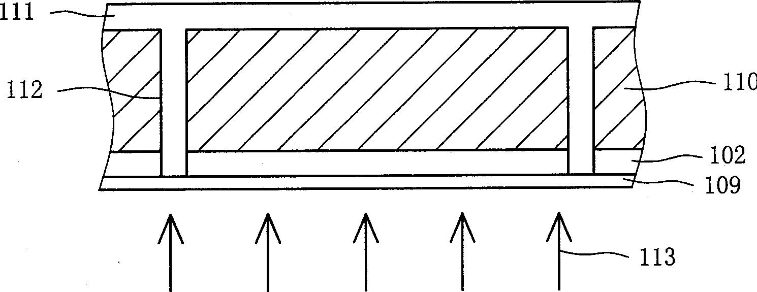
[0039] Figure 6A 6F is a manufacturing method of an array color flat panel display structure according to a preferred embodiment of the present invention. Please refer to Figure 6A Firstly, a first electrode 602 and a sacrificial layer 604 are sequentially formed on a transparent substrate 601, wherein the sacrificial layer 604 can be made of a transparent material, such as a dielectric material, or an opaque material, such as a metal material. Openings 606, 608, 610, 612 are formed in the first electrode 602 and the sacrificial layer 604 by a lithographic etching process, and the openings 606, 608, 610, 612 are suitable for forming supports therein.

[0040] Next, a material layer 614 is formed on the sacrificial layer 604 and fills the openings 606 , 608 , 610 , 612 . Two of the four openings 606 , 608 , 610 , 612 define the positions of the light-emitting interferometric display units 630 , 632 , and 634 . The material layer 614 is suitable for forming a support, gener...


PUM


Abstract

The light interference type display unit structure includes one first electrode and one second electrode supported by some supporting matter. The present invention features that the second electrode in different thickness has different stress so that the second electrode is shifted in the thermal process and the distance between the first electrode and the second electrode is altered. The manufacture process of the light interference type display unit includes successively forming the first electrode and the sacrificial layer on the substrate; forming opening in the first electrode and the sacrificial layer; defining the support inside the opening with at least one support top arm located on the sacrificial layer; forming the second electrode in different thickness over the sacrificial layer and the support; performing one thermal process; and finally removing the sacrificial layer to obtain the light interference type display unit.

Description

technical field [0001] The invention relates to a method for manufacturing an optical interference display panel, in particular to a method for manufacturing an optical interference display panel with a support of a support arm. Background technique [0002] Due to the characteristics of small size and light weight, the flat panel display has great advantages in the portable display device and the display market for small space applications. In addition to liquid crystal displays (Liquid Crystal Display, LCD), organic electro-luminescent diodes (Organic Electro-Luminescent Display, OLED) and plasma displays (Plasma Display Panel, PDP), etc., today's flat-panel displays use light interference A flat display mode has been proposed. [0003] Please refer to US Patent No. USP5835255, which discloses a visible light display unit array (Array of Modulation), which can be used as a flat panel display. See figure 1 , figure 1 It is a schematic cross-sectional view of a known dis...

Claims


Application Information

Patent Timeline
Patent Type & Authority Applications(China)
IPC IPC(8): G02B26/06G02F1/03G02F1/17G02F1/21G03F7/00H01L21/3205
Inventor 林文坚
Owner IDC LLC
Why Eureka
Try Eureka