Active matrix type display device
A display and strip source technology, which is applied in the field of electronic devices equipped with the electro-optical device, can solve the problems such as the drop of the holding voltage, the decrease of the contrast quality of the displayed image, and the change of the electro-optical characteristics of the liquid crystal.
- Summary
- Abstract
- Description
- Claims
- Application Information
AI Technical Summary
Problems solved by technology
Method used
Image

Examples
no. 1 example
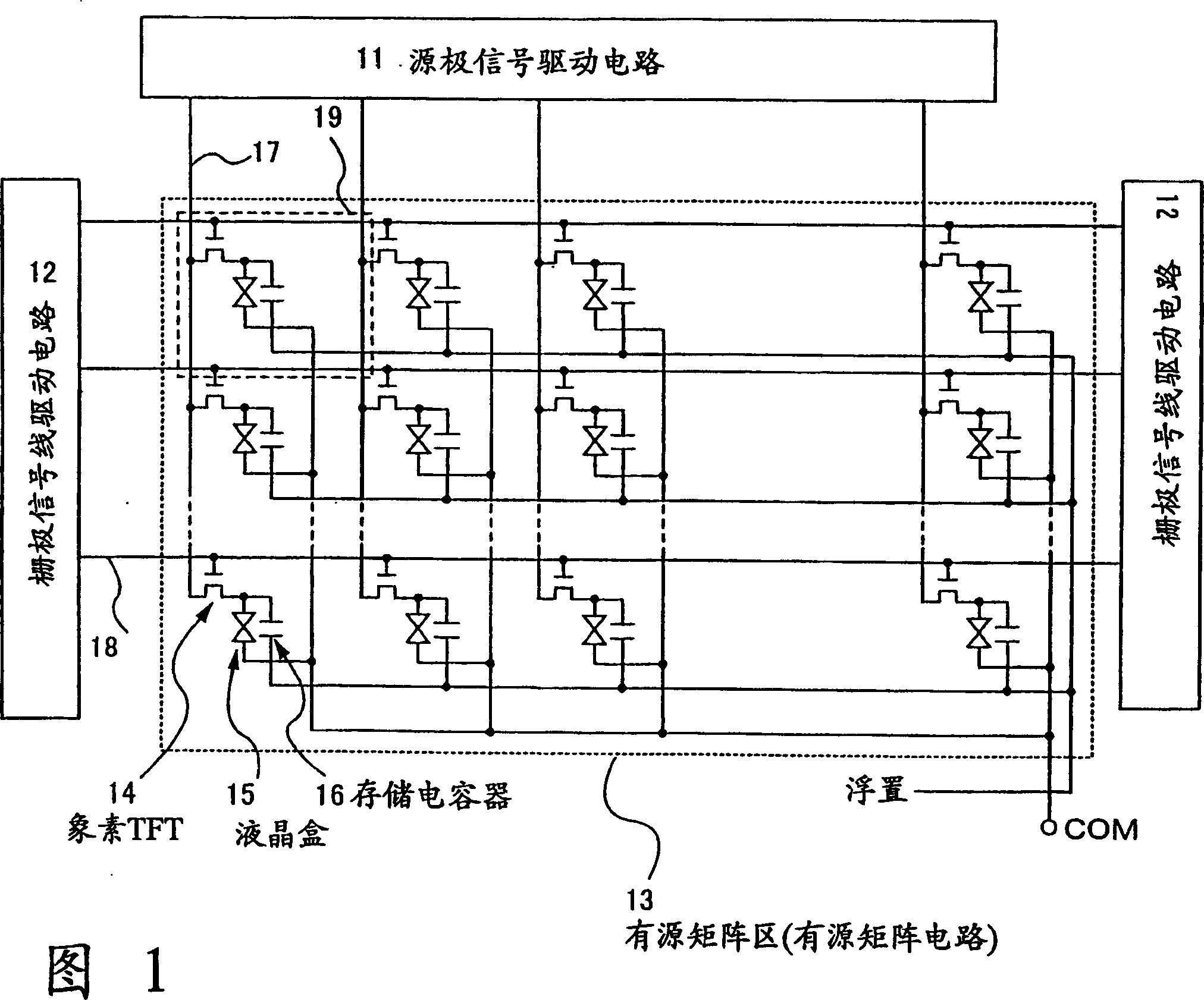
[0161] An example of an active matrix liquid crystal display to which the present invention is applied will be described below using FIG. 1 .
[0162] Fig. 1 shows an example of a circuit diagram of an active matrix circuit using a holding capacitor of the present invention. The active signal line driving circuit 11 shown in Fig. 1, the gate signal line driving circuit 12, the active matrix circuit 13, the pixel thin film transistor 14, the liquid crystal cell with liquid crystal sandwiched between the pixel electrode and the opposite electrode 15. A holding capacitor 16, a source signal line 17 and a gate signal line 18 formed by sandwiching a dielectric between a pixel electrode and a shielding film. The source signal line driver circuit 11 and the gate signal line driver circuit 12 are generally called driver circuits. These driver circuits are formed on the same substrate as the pixel matrix region including the active matrix circuits.
[0163] In the active matrix regio...
no. 2 example
[0231] In addition to the structure in which the shielding film is floated in the first embodiment, an example in which a large-capacity coupling capacitor is formed between the shielding film and the common line will be described in this embodiment.
[0232] Fig. 11 is an example of a circuit diagram of an active matrix circuit using a holding capacitor according to the present invention. As shown in FIG. 11, a source signal line driver circuit 301, a gate signal line driver circuit 302, an active matrix circuit 303, and a pixel thin film transistor 304 are provided, and a liquid crystal is sandwiched between the pixel electrode and the opposite electrode. A liquid crystal cell 305, a holding capacitor 306 formed by sandwiching a dielectric between a pixel electrode and a shielding film, a source signal line 307, and a gate signal line 308. A coupling capacitor 310 is also provided between the shield film in the floating state and the common line. The source signal line driv...
no. 3 example
[0254] In addition to the method shown in Embodiment 1, an example of a method of manufacturing a thin film transistor of a pixel matrix circuit and a driver circuit provided therearound will be described below with reference to FIGS. 13 to 15. The method disclosed in this embodiment can also be used to manufacture the semiconductor device of the present invention.
[0255] [Step of forming island-shaped semiconductor layer and gate insulating film: FIG. 13A ]
[0256] In FIG. 13A, a non-alkaline glass substrate or a quartz substrate is preferably used as the substrate 7001. Besides, it may be a silicon substrate or a metal substrate on which an insulating film is formed.
[0257] On the surface of a substrate 7001 on which thin film transistors are formed by plasma CVD or sputtering, an underlayer film made of a silicon oxide film, a silicon nitride film, or a silicon oxynitride film is formed to a thickness of 100 nm to 400 nm. The underlayer film 7002 may be a two-layer s...
PUM
| Property | Measurement | Unit |
|---|---|---|
| thickness | aaaaa | aaaaa |
| thickness | aaaaa | aaaaa |
| thickness | aaaaa | aaaaa |
Abstract
Description
Claims
Application Information
PatSnap Eureka turns technology decisions into work you can execute. Powered by our Innovation Knowledge Graph, it runs expert workflows across engineering, life sciences, materials and intellectual property. Get your review-ready output in minutes.


