Light-emitting component capable of increasing light-emitting active area

A technology of light-emitting element and active area, which is applied in the direction of electrical components, semiconductor devices, circuits, etc., can solve the problems of reducing the amount of light output, light-emitting brightness, occupation, etc.

Inactive Publication Date: 2004-12-29
OPTO TECH
View PDF0 Cites 4 Cited by
  • Summary
  • Abstract
  • Description
  • Claims
  • Application Information

AI Technical Summary

Problems solved by technology

Therefore, the second connection electrode 293 occupies a part of the area of ​​the light-emitting action area 253, which relatively causes the regret of reducing the amount of light output and the brightness of light emission.

Method used


Image

  • Light-emitting component capable of increasing light-emitting active area
  • Light-emitting component capable of increasing light-emitting active area
  • Light-emitting component capable of increasing light-emitting active area

Examples


Embodiment Construction

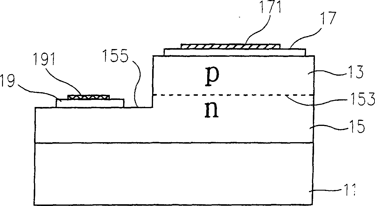
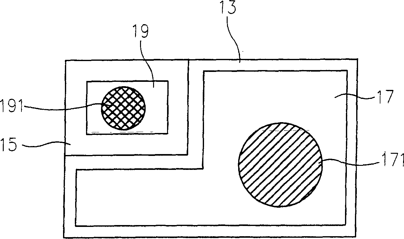
[0044] First, see Figure 3A to Figure 3C , are respectively a top view of the structure of a preferred embodiment of the present invention, a schematic cross-sectional view along line C-D, and a top view of the structure of the power supply substrate. As shown in the figure, the LED element that can increase the light-emitting active area is mainly composed of an LED chip 30 and a power supply substrate 41 . Wherein, the LED die 30 mainly forms a second epitaxial layer 35 on a die substrate 31, and the second epitaxial layer 35 can define a relatively convex first surface 353 and a relatively concave second surface. surface 355 , and a first epitaxial layer 33 is formed above the first surface 353 , so that a light-emitting region (namely the first surface 353 ) is naturally formed between the first epitaxial layer 33 and the second epitaxial layer 35 . Generally, the grain substrate 31 can be made of silicon carbide, gallium arsenide, sapphire, gallium nitride and other mat...


PUM


Abstract

The invention relates to a light-emitting component, in particular a light-emitting component for increasing light-emitting active region and raising luminescent brightness, wherein a second epitaxy layer and at least a first epitaxy layer are arranged on a crystal particle substrate, the upper surface of the first epitaxy is provided with at least a first electrode, a plurality of second electrodes insulated by the first electrode insulating layer and electrically connected to the second epitaxy layer, the first electrode and the second electrodes are in staggered arrangement.

Description

technical field [0001] The present invention relates to a light-emitting element, especially a light-emitting element that can increase the area of ​​the light-emitting action area to increase the luminous brightness. The main method is to arrange a first connecting circuit and a second connecting circuit on a power supply substrate, and Does not directly occupy the light-emitting active area of ​​the light-emitting diode. Background technique [0002] Light-emitting diodes are widely used in computer peripherals, communication products, and other electronic devices due to their advantages of small size, light weight, low power consumption, and long life. Generally mass-produced light-emitting diodes are grown on a substrate, such as sapphire (sapphire), silicon carbide (SiC) and other materials, to grow an epitaxial layer with a pn junction. When a driving voltage is introduced on both sides of the layer, the pn junction can project a light source due to electron-hole reco...

Claims


Application Information

Patent Timeline
Patent Type & Authority Applications(China)
IPC IPC(8): H01L33/00
Inventor 林明德林三宝许荣贵
Owner OPTO TECH
Why Eureka
Try Eureka