Microstructure manufacturing method combining light hardening molding

A manufacturing method and microstructure technology, applied in directions such as printing, can solve the problems of rough inner walls of pores 61, increased ink resistance, poor precision, etc., so as to save procedures and time, improve precision, and save mold repairs. or the effect of correction

Inactive Publication Date: 2005-01-19
郭佳儱 +2
View PDF0 Cites 4 Cited by
  • Summary
  • Abstract
  • Description
  • Claims
  • Application Information

AI Technical Summary

Problems solved by technology

[0003] The first is to use laser processing to drill holes, and the shortcoming of this existing processing method is that the inner wall of the fine hole 61 is relatively rough, and those who are familiar with this technology, the special ink of inkjet printer, its ink liquid is slightly It tends to be thicker, which greatly improves the viscosity (or adhesion) of the liquid to the rougher contact surface.
Therefore, if the surface of the inner wall of the fine hole 61 for ink jet flow is not fine enough and the precision is not good enough, the resistance to ink flow will be increased virtually, and when the printer is used for inkjet printing with higher resolution , due to the substantial increase in the amount of ink ejected, it is easy to cause the pores 61 of the existing structure to be clogged when the jet flow is not good enough
Secondly, since the laser can only be carried out in a straight line, the fine holes 61 processed can only be vertical walls, and the fine holes 61 with arc surfaces or special geometric shapes cannot be produced, so it is impossible to manufacture special flow channels or hole shapes. microstructure products
[0004] The second existing method is to use copper electroforming micro-holes, but as we all know, laser processing is "optical processing", and the precision must be higher than that of copper electroforming. Copper electroformed micropores still face various processing quality problems such as inaccurate micropore size, poor precision and rough surface. Especially for the processing conditions of micropore diameter less than 50 microns, the existing processing technology is almost impossible to complete.

Method used


Image

  • Microstructure manufacturing method combining light hardening molding
  • Microstructure manufacturing method combining light hardening molding
  • Microstructure manufacturing method combining light hardening molding

Examples


Embodiment Construction

[0036] The present invention is a microstructure manufacturing method combined with photohardening molding, and mainly relates to a method for manufacturing a high-precision microstructure sheet, and the application of the microstructure sheet to a printer can improve the precision of the jet flow. Spend.

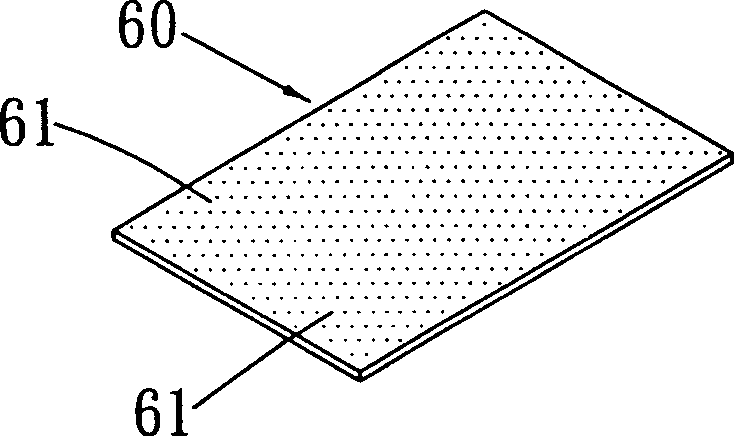
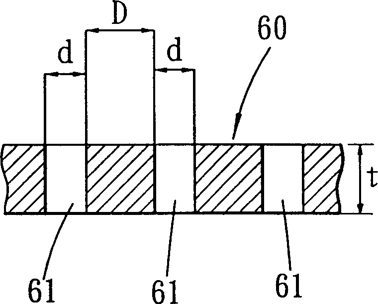
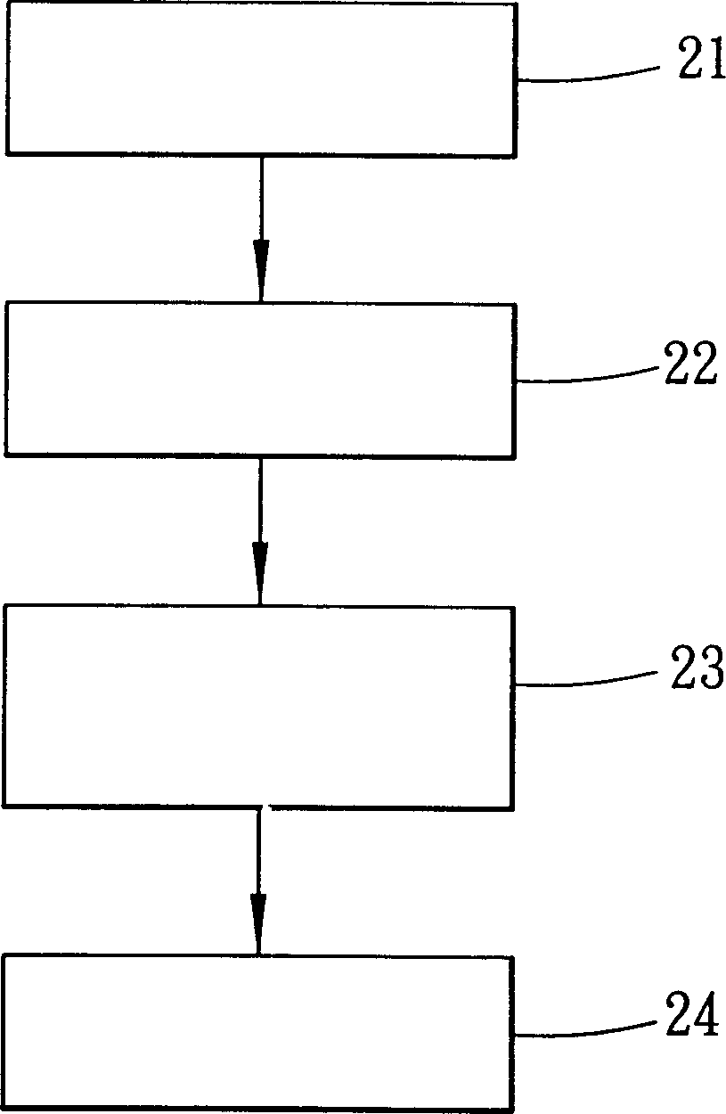
[0037] In this embodiment, the microstructure sheet 16 is about 7 mm long, 4 mm wide, and 50 microns thick, and at least one fine hole 161 is formed through the microstructure sheet 16 (the preferred embodiment of the present invention is several ); and the present invention is made according to the following steps, please refer to image 3 The flow chart shown is for illustration:

[0038] 1. Pre-step 21:

[0039] Such as Figure 4A As shown, make a bottom mold structure 10 earlier, form at least one mold body 11 (simplified to three in the figure of the preferred embodiment of the present invention to represent thousands or several Wangen), the mold body 11 can be con...


PUM

PropertyMeasurementUnit
thicknessaaaaaaaaaa

Abstract

A microstructure manufacturing method combining with photohardening at least includes the following steps: 1. preparing; 2. spraying glue liquid; 3. exposing to ultraviolet light; 4. removing the bottom die. By spraying liquid state glue and solidifying with the ultraviolet radiation, a finished precise microstructure can be obtained. The microstructure can be non-penetrative micro-texture or microstructure, or micro-perforated flake, and can be used for micro-optical lens array, micro-optical diffraction element, ink-jet printer, biological wafer reagent or fuel cell commutation pore or relative nanometer technology. At the same time, the method can make the pores form special geometric shape and greatly reduce the procedure and time of repairing die or correction.

Description

technical field [0001] The invention relates to a microstructure manufacturing method combined with photohardening molding. Background technique [0002] The scientific and technological "noun" of nanometer has become familiar to people in today's era of rapid technological advancement and has a wide range of applications. see figure 1 and figure 2 For example, the nozzle sheet 60 applied to the nozzle of an inkjet printer at the present stage is an example. The nozzle sheet 60 is a three-dimensional rectangle with a length of 7 mm, a width of 4 mm, and a thickness (t) of 50 microns. The nozzle sheet 60 is formed vertically. Several fine holes 61, the diameter (d) of the fine holes 61 is 100 microns, and the hole distance (D) is 100 to 200 microns. Since the diameter (d) of the fine hole 61 is very small, it cannot be completed with the precision of the existing drilling and cutting technology. And except existing cutting technology, existing production method that can ...

Claims


Application Information

Patent Timeline
Patent Type & Authority Applications(China)
IPC IPC(8): B41J2/16
Inventor 郭佳儱曾世昌
Owner 郭佳儱
Why Eureka
Try Eureka