Junction field effect transistor

A field effect transistor and junction gate technology, applied in the field of microelectronic semiconductors, can solve the problems of high driving current electrical characteristics, low leakage current, etc., and achieve the effects of good heat dissipation efficiency, cost saving, and suitable for large-scale integration

Inactive Publication Date: 2005-03-23
SEMICON MFG INT (SHANGHAI) CORP +1
View PDF0 Cites 2 Cited by
  • Summary
  • Abstract
  • Description
  • Claims
  • Application Information

AI Technical Summary

Problems solved by technology

[0003] The present invention overcomes the structural defects of the above-mentioned field effect transistors, and provides a junction-gate field effect transistor, which can not only obtain the electrical characteristics of a very low leakage current and a high driving current, but also solve the problem of the gate oxide of the device at the nanometer scale. problems and has good heat dissipation performance, which further improves the large-scale integration of devices

Method used


Image

  • Junction field effect transistor
  • Junction field effect transistor
  • Junction field effect transistor

Examples


Embodiment Construction

[0019] Specific implementation examples

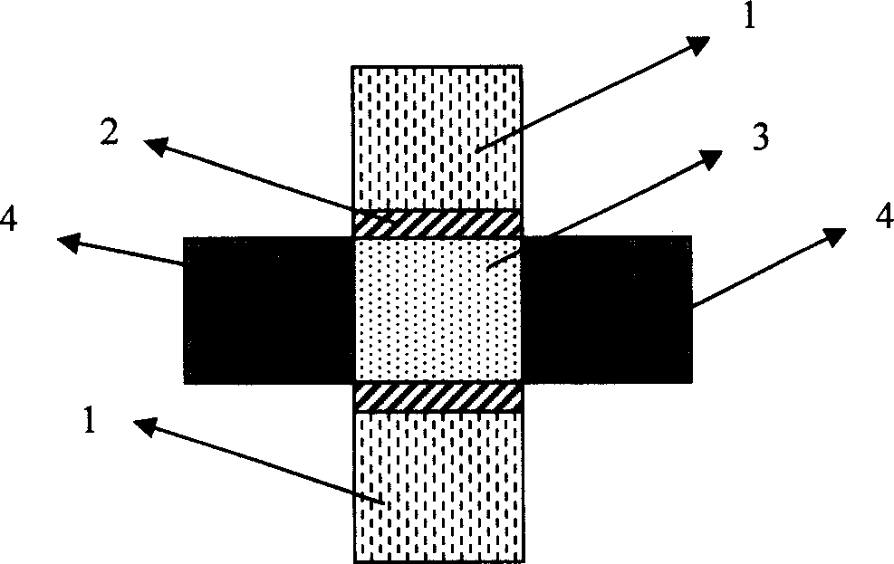
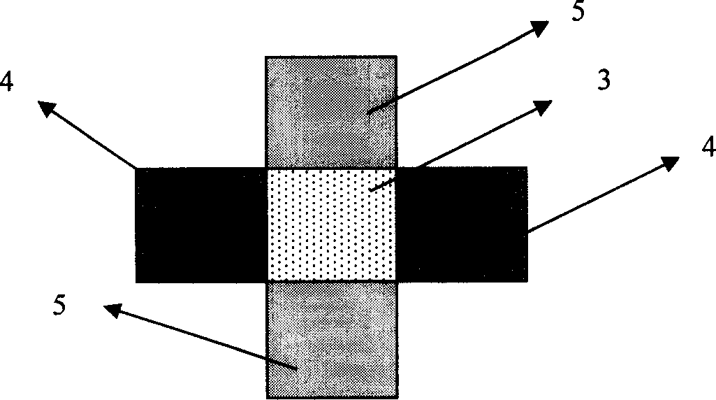
[0020] refer to figure 2 , the dual gate junction gate field effect transistor of the present invention comprises: source region 4, drain region 4, double control gate 5 and body 3, body 3 is square, control gate 5 is doped monocrystalline silicon, control gate and body are directly connected Form a P-N junction, the body is a square. It can be seen from the figure that the dual-gate junction gate field effect transistor of the present invention is a completely symmetrical structure, so as long as the connecting electrodes between the control gate and the source and drain are changed, the n-type double gate junction gate field effect transistor and the p-type double gate field effect transistor.

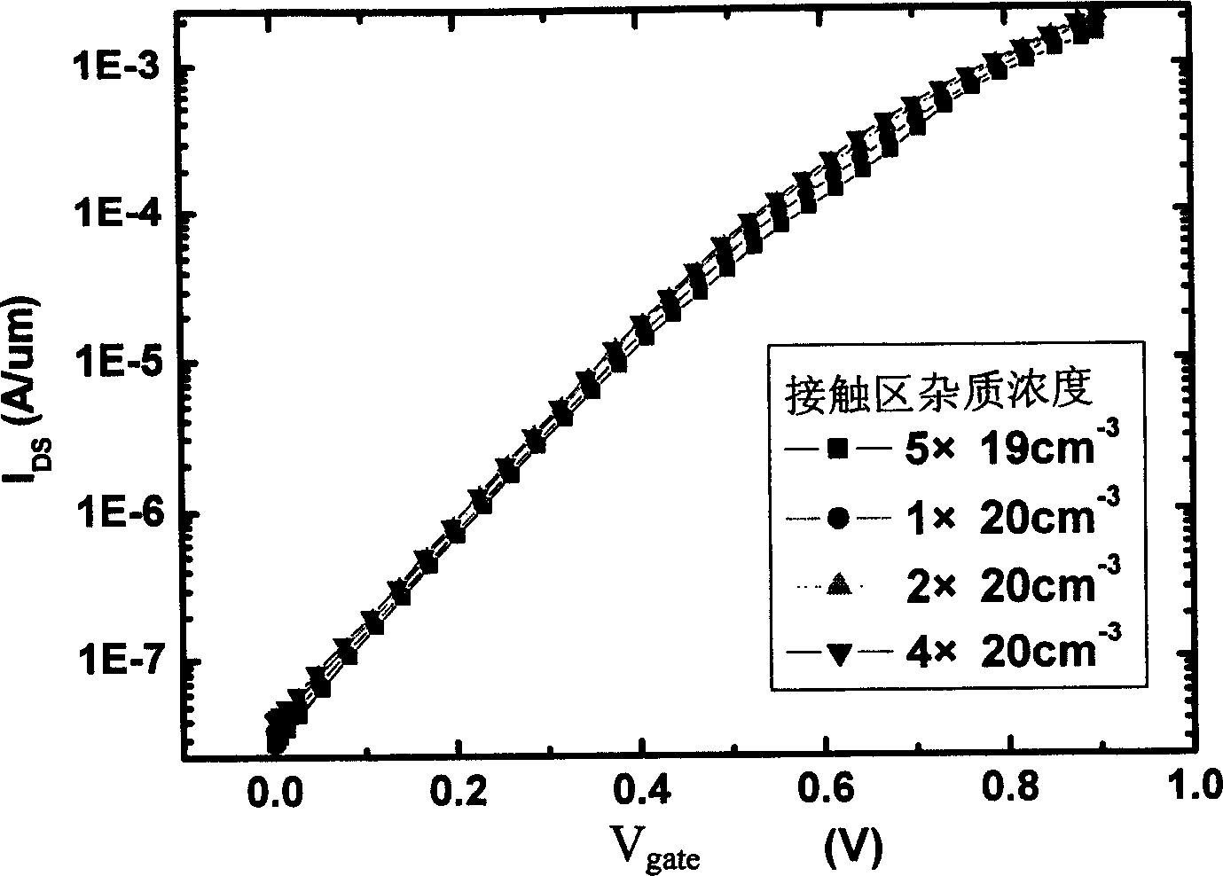
[0021] The specific implementation example of the double-gate junction gate field effect transistor of the present invention, taking the side length of the body as an example, its specific design structural parameters are as follows: the l...


PUM


Abstract

The invention provides a junction grid field effect transistor and belongs to the field of the micro-electronic semiconductor technology. The junction grid field effect transistor includes the source region, drain region, body and control grid. The control grid is the adulterated single crystal of silicon and connects with the body to form the P-N junction. Different from the structure of the traditional field effect transistors, the structure of the metal-insulating layer-semiconductor, the invention gets rid of the grid oxygen in the normal device and realizes the structure of semiconductor-semiconductor. Without the isolation of the grid oxygen, the device of the invention has good heat radiating property and is pretty adaptable to large scale and high density integration. Because the body is foursquare and the structure of the device is symmetrical, the dual junction gate field effect transistors are based on the n-type field effect transistor and p-type field effect transistor.

Description

technical field [0001] The invention belongs to the technical field of microelectronics and semiconductors, and in particular relates to a junction gate field effect transistor. Background technique [0002] With the continuous development of microelectronics technology, the density of circuit integration is increasing, the size of devices is becoming smaller and smaller, and the difficulty of integration is also increasing. Especially after decades of rapid development, the size of microelectronic devices has entered the nanoscale. Many effects that only appear in small sizes seriously threaten the development of devices, and then affect the progress of the entire microelectronics technology. For example, with the continuous shrinking of the device size, the preparation of high-quality thin-layer gate oxide is an insurmountable difficulty in the current technology. Although there are many alternative technologies, such as high-K dielectric (Oates et al., IEDM Tech.Dig., p...

Claims


Application Information

Patent Timeline
Patent Type & Authority Applications(China)
IPC IPC(8): H01L29/772
Inventor 陈刚黄如张兴王阳元
Owner SEMICON MFG INT (SHANGHAI) CORP
Why Eureka
Try Eureka