Structure of shallow ridge isolation area and dynamic DASD and its mfg method

A technology of dynamic random access and shallow trench isolation, which is applied in semiconductor/solid-state device manufacturing, electrical components, transistors, etc., can solve problems such as junction leakage and improvement, and achieve the effect of improving uniformity and avoiding gradient improvement

Active Publication Date: 2005-03-30
PROMOS TECH INC
View PDF1 Cites 1 Cited by
  • Summary
  • Abstract
  • Description
  • Claims
  • Application Information

AI Technical Summary

Problems solved by technology

However, this will make the p-type implant region 130 closer to the buried doped strip 110. In this case, if the starting voltage of the parasitic transistor is to be increased to increase the doping conce...

Method used


Image

  • Structure of shallow ridge isolation area and dynamic DASD and its mfg method
  • Structure of shallow ridge isolation area and dynamic DASD and its mfg method
  • Structure of shallow ridge isolation area and dynamic DASD and its mfg method

Examples


Embodiment Construction

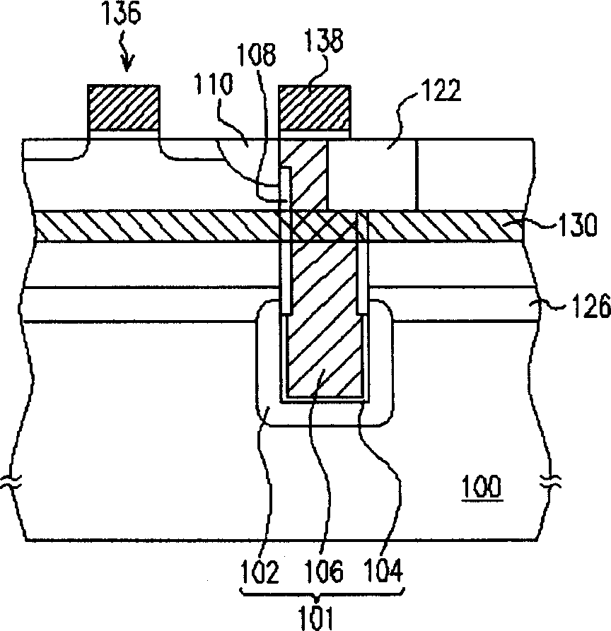
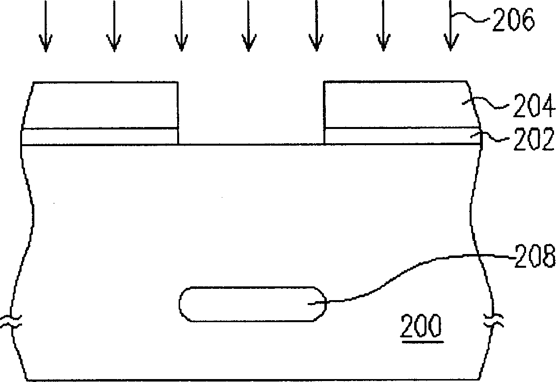
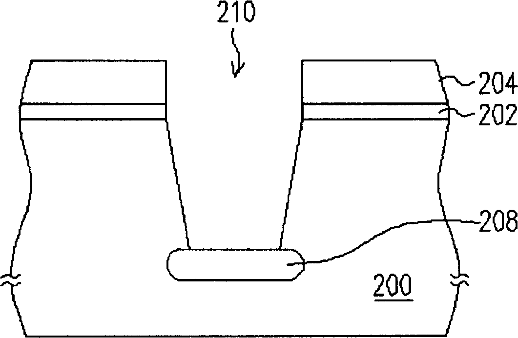
[0035] Figure 2A to Figure 2C As shown, it is a schematic cross-sectional view of a manufacturing process of a shallow trench isolation region according to a preferred embodiment of the present invention. Please refer to Figure 2A First, a pad oxide layer 202 and a mask layer 204 are formed on a substrate 200 . Wherein, the pad oxide layer 202 is used to protect the surface of the substrate 200, and the thickness of the mask layer 204 is, for example, greater than 600 angstroms, which may be a silicon nitride layer, a stacked layer of a silicon nitride layer / photoresist layer , or a stacked layer of silicon nitride layer / silicon oxide layer / photoresist layer, depending on the process requirements. The method for forming the mask layer 204 and the pad oxide layer 202 is, for example, to first form an oxide thin layer (not shown) on the surface of the substrate 200, and then form a mask material layer (not shown) on the oxide thin layer, After forming a patterned photoresis...


PUM

PropertyMeasurementUnit
Thicknessaaaaaaaaaa

Abstract

First, patterned mask layer is formed on a substrate. Next, an ion-implantation step is carried out in order to form a doping range on substrate uncovered by mask layer. Then, an etching step is carried out in order to patternize substrate. Thus, a groove is formed on the substrate, and doping area is exposed at bottom of groove. A insulating layer is filled into the groove to form a shallow groove isolation region. In the invention, doping area is formed at bottom of shallow groove isolation region, and not formed at side wall.

Description

technical field [0001] The present invention relates to a structure of a semiconductor element and a manufacturing method thereof, and in particular to a structure of a shallow trench isolation region and a dynamic random access memory and a manufacturing method thereof. Background technique [0002] When semiconductors enter the deep sub-micron (Deep Sub-Micron) process, the size of the components gradually shrinks. For the previous DRAM structure, it means that the space for capacitors is getting smaller and smaller. On the other hand, Due to the increasingly large computer application software, the memory capacity required is also increasing. For this situation where the size of the memory is reduced but the memory capacity needs to be increased, it shows that the manufacturing method of the capacitor of the previous dynamic random access memory must be Changed to fit the trend. [0003] Dynamic random access memory (DRAM) can be mainly divided into two forms according t...

Claims


Application Information

Patent Timeline
IPC IPC(8): H01L21/76H01L21/8242H01L27/108
Inventor 李岳川陈世芳
Owner PROMOS TECH INC
Why Eureka
Try Eureka