Semiconductor light emitting device and manufacturing method for the same

A technology for light-emitting devices and semiconductors, which is applied to the structural details of semiconductor devices, semiconductor lasers, and semiconductor lasers. , the effect of avoiding characteristic deterioration

Inactive Publication Date: 2005-03-30
SHARP KK
View PDF1 Cites 5 Cited by
  • Summary
  • Abstract
  • Description
  • Claims
  • Application Information

AI Technical Summary

Problems solved by technology

Therefore, in the case of using solder foil, the heat generated in the laser chip cannot be effectively dissipated to the support base, resulting in deterioration of characteristics when the temperature of the light emitting part rises
In addition, the laser chip according to the above method is easy to move during mounting, which causes a problem when the mounting angle of the mounted laser chip varies greatly

Method used


Image

  • Semiconductor light emitting device and manufacturing method for the same
  • Semiconductor light emitting device and manufacturing method for the same
  • Semiconductor light emitting device and manufacturing method for the same

Examples


no. 1 example

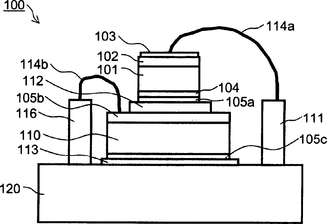
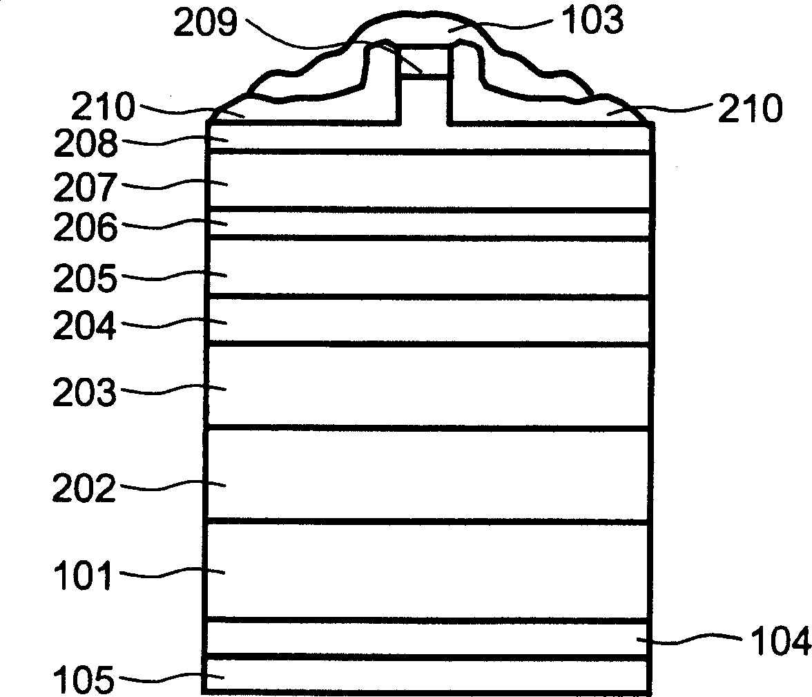
[0023] FIG. 1 is a side view of a semiconductor laser device 100 according to a first embodiment. In FIG. 1 , a nitrogen-based semiconductor layered body 102 is formed on a GaN substrate 101 . Furthermore, p-electrode 103 is provided on the upper surface of nitrogen-based semiconductor layered body 102 , and n-electrode 104 and multilayer metal film 105 a for metallization are provided under the lower surface of GaN substrate 101 .

[0024] The basic structure of the semiconductor laser chip used in the semiconductor laser device 100 according to the first embodiment is as described above, and its details will be described below.

[0025] Via heat spreader 110 , the semiconductor laser chip is protected and layered on support base 120 . The semiconductor laser chip is connected to the heat sink 110 together with the p-electrode 103 facing upward via the solder 112 and the multilayer metal film 105b. Then, the heat sink 110 is connected to the support base 120 via the multila...

no. 2 example

[0044] By changing the material of the solder 113 transcribed to the support base 120 in the semiconductor laser device according to the first embodiment to SnAgCu, the semiconductor laser device according to the second embodiment is obtained. The same numerals denote the same constituent parts as those of the first embodiment, except that numeral 113a denoting the above-mentioned solder is used to describe the second embodiment.

[0045] A Teflon tape with a length of 500 mm and a width of 600 μm was prepared, and the SnAg 0.03 Cu 0.005 Deposited from the vapor form onto a Teflon tape to have a thickness of about 8 μm. Subsequently, the Teflon tape on which the SnAgCu solder 113 a is deposited is placed relative to the supporting base 120 . After placement, ultrasonic vibration of about 80 kHz was applied to the solder 113 a through the Teflon tape, so that the solder 113 a having dimensions of 500 μm length×500 μm width×8 μm thickness was transcribed onto the supporting ba...


PUM


Abstract

An object of the present invention is to provide a semiconductor light emitting device having a long lifespan by improving yield in mounting. In order to achieve this object, a semiconductor light emitting device includes a semiconductor light emitting element chip having an n-type GaN substrate, a heat sink made of SiC onto which the semiconductor light emitting element chip is mounted, a solder made of AuSn which joins the n-type GaN substrate to the heat sink, a support base onto which the heat sink is mounted, and a solder made of In or SnAgCu which joins the heat sink to the support base. The solder has a thickness in a range from 1 mum or more to 20 mum or less, and the heat sink has a thickness in a range from 100 mum or more to 500 mum or less.

Description

technical field [0001] The invention relates to a semiconductor light emitting device (including a semiconductor laser device) and a manufacturing method thereof. More specifically, the present invention relates to a semiconductor light emitting element chip mounting and heat sink mounting. Background technique [0002] A semiconductor laser device has a laser chip including an active layer made of nitrogen-based semiconductors typified by GaN, InN, AlN and mixed crystals of these semiconductors have been fabricated as prototypes. A laser element made of a nitrogen-based semiconductor has a high operating voltage, and a driver for driving the laser has a low driving voltage. Therefore, to use such a driver, a floating type laser is applied, and it is also necessary to insert and install an insulating heat sink between the laser and a support base. [0003] In a conventional assembly of a semiconductor laser device, a laser chip is mounted on a heat sink, and then, a sheet-...

Claims


Application Information

Patent Timeline
Patent Type & Authority Applications(China)
IPC IPC(8): H01S5/022H01L23/00H01L29/22H01S5/00H01S5/02H01S5/024H01S5/042H01S5/223H01S5/323H01S5/343
CPCH01L2924/01021H01L2924/01046H01S5/02476H01L2924/01079H01L33/62H01L2924/12041B82Y20/00H01L2924/01063H01S5/02272H01L33/641H01S5/34333H01S5/2231H01L2924/01078H01L2924/01057H01L2224/48091H01S5/0021H01L2224/73265H01L2924/01077H01S5/0237H01L2924/00014
Inventor 石田真也
Owner SHARP KK
Why Eureka
Try Eureka