Structure of LED and its mfg method

A technology of light-emitting diodes and manufacturing methods, which is applied in the direction of electrical components, circuits, semiconductor devices, etc., can solve problems such as complicated manufacturing processes, and achieve the effects of reducing volatilization, stabilizing voltage, and optimizing current distribution

Active Publication Date: 2005-03-30
EPISTAR CORP
View PDF0 Cites 23 Cited by
  • Summary
  • Abstract
  • Description
  • Claims
  • Application Information

AI Technical Summary

Problems solved by technology

However, the disadvantage of this TS AlGaInP LED is that the manufacturing process is too complicated, and it usually has a high resistance characteristic of a non-ohmic contact at the bonding interface

Method used


Image

  • Structure of LED and its mfg method
  • Structure of LED and its mfg method
  • Structure of LED and its mfg method

Examples


Embodiment Construction

[0042] The invention discloses a light emitting diode structure and a manufacturing method thereof.

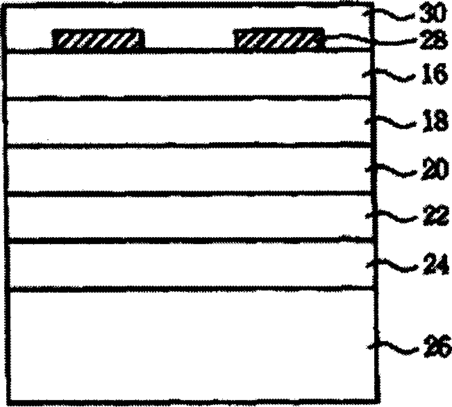
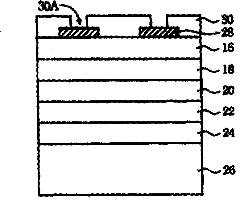
[0043] Such as Figure 1A As shown, the epitaxial structure of the light-emitting diode of the present invention includes an N-type gallium arsenide (GaAs) substrate 26, an etching stop layer (Etching Stop Layer) 24, an N-type aluminum gallium indium phosphide (AlxGa1-x) stacked in sequence. 0.5In0.5P lower cladding (Cladding) layer 22 and aluminum gallium indium phosphide (AlxGa1-x) 0.5In0.5P active layer (Active Layer) 20, P-type aluminum gallium indium phosphide (AlxGa1-x) 0.5 An upper cladding layer 18 of In0.5P and a P-type Ohmic Contact Epitaxial Layer (Ohmic Contact Epitaxial Layer) 16 . Next, a P-type ohmic contact metal electrode layer (first ohmic contact metal electrode layer) 28 is formed on the P-type ohmic contact epitaxial layer 16 by conventional techniques. Subsequently, a mirror protection layer 30 is deposited thereon, and the above-mentioned mirror protec...


PUM


Abstract

Metal base plate with high conductivity and high reflectance is adopted in the invention instead of traditional extinctive gallium arsenide base plate, and after diodes are made, two adjacent LED are connected in series through semiconductor fabricating process. Mirror protective layer is adhibited in order to protect metal reflecting layer p and n poles, in which one is higher and the other is lower, of epitaxy chip of LED so as to form LED with p and n poles being at same side. Trench at joint place between two adjacent epitaxy chips of LED is etched out, and a dielectric layer is filled into the trench in order to protect sidewall of adjacent LED. The invention raises luminous efficiency of LED, and increases luminous intensity.

Description

Technical field: [0001] The invention relates to a structure of a light emitting diode (Light Emitting Diode; LED) chip and a manufacturing method thereof. In particular, it relates to the structure and manufacturing method of aluminum gallium indium phosphide (AlGaInP) and aluminum gallium arsenide light-emitting diodes with p and n electrodes in the same direction. Background technique: [0002] The traditional aluminum gallium indium phosphide light-emitting diode has a double heterostructure (Double Heterostructure; DH). A lower cladding layer 4 of n-type (AlxGa1-x) 0.5In0.5P at 70%-100%, an active layer 5 of (AlxGa1-x)0.5In0.5P, an aluminum content of 70%-100% A p-type (AlxGa1-x) 0.5In0.5P upper cladding layer 6, and a p-type high energy gap current spreading layer (Current Spreading Layer) 7, the material of this layer can be gallium phosphide, gallium arsenide phosphide , indium gallium phosphide or aluminum gallium arsenide, etc. [0003] Then, by changing the com...

Claims


Application Information

Patent Timeline
Patent Type & Authority Applications(China)
IPC IPC(8): H01L33/00
Inventor 林锦源杜全成
Owner EPISTAR CORP
Why Eureka
Try Eureka