Surface acoustic wave element and method for fabricating semiconductor device

A surface acoustic wave and manufacturing method technology, applied to electrical components, impedance networks, etc., can solve problems such as low productivity

Inactive Publication Date: 2005-05-25
NEC CORP
View PDF0 Cites 1 Cited by
  • Summary
  • Abstract
  • Description
  • Claims
  • Application Information

AI Technical Summary

Problems solved by technology

However, the resist pattern is formed by electron beam exposure, because the electron beam is used to draw along the pattern on the resist, so compared with the photolithography technology that can be exposed in batches, there is a disadvantage of lower productivity.
And because of its extremely high precision, the thermal expansion and contraction of the substrate due to external temperature changes cannot be ignored, resulting in errors caused by time-dependent changes in the drawing patterns of each substrate, and the yield is also a problem.

Method used


Image

  • Surface acoustic wave element and method for fabricating semiconductor device
  • Surface acoustic wave element and method for fabricating semiconductor device
  • Surface acoustic wave element and method for fabricating semiconductor device

Examples


Embodiment Construction

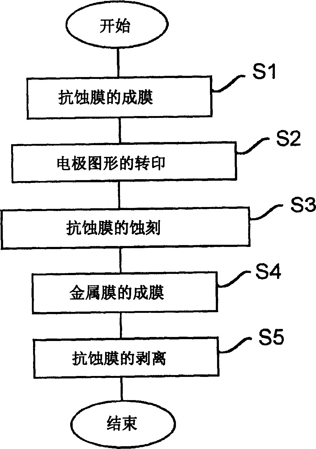
[0026] Hereinafter, embodiments of the present invention will be described with reference to the drawings.

[0027] refer to figure 1 and Figure 2A ~ Figure 2F A method of manufacturing a surface acoustic wave element will be described.

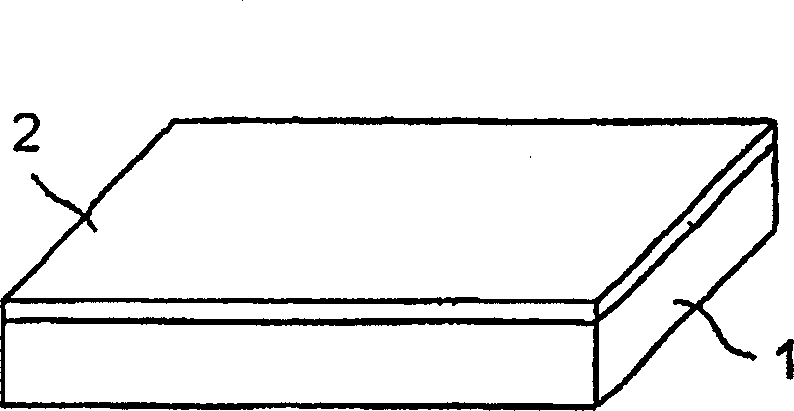
[0028] First, if Figure 2A As shown, a flat resist film 2 is formed on the piezoelectric substrate 1 by the spin coating method (step S1). As the piezoelectric substrate 1, a single crystal piezoelectric substrate such as LiTiO3, LiNbO3, or crystal, a substrate on which an insulating film is formed, a substrate composed of a ceramic piezoelectric body such as PZT or PLZT, or a substrate laminated on a substrate can be preferably used. Thin film substrates such as diamond thin films and ZnO thin films.

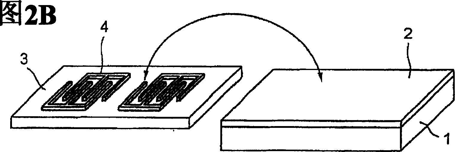
[0029] Next, as shown in FIG. 2B , the template 3 on which the curtain-like fine electrode pattern 4 is formed is pressed against the surface of the substrate 1 . In this way, if Figure 2C As shown, the curtain-shaped micro-electrode ...


PUM


Abstract

A method for manufacturing surface acoustic wave elements and semiconductor devices, in which a template (3) with high-precision concavities and convexities manufactured in advance by photolithography technology using electron beams is pressed onto a substrate (1) coated with a resist film (2) ), transfer the resist pattern (5). Then, on the resist film pattern (5) formed by transfer printing, a metal thin film (6) is formed and peeled off together with the resist film (2) by a lift-off method.

Description

technical field [0001] The present invention relates to a method of manufacturing a surface acoustic wave element and a semiconductor device, and in particular, to a method of manufacturing an element capable of mass-producing an element whose operating frequency and operating wavelength can be determined with high precision even in high-frequency and short-wave regions at low cost. Background technique [0002] Surface acoustic wave devices are devices that generate surface acoustic waves on the surface of the substrate by using curtain electrodes formed on a piezoelectric substrate. They are widely used as bandpass filters and resonators in the field of wireless communications. Especially when used as a bandpass filter, compared with dielectric filters and laminated LC filters, it has the characteristics of being smaller and can quickly remove out-of-band signals. Therefore, the use of surface acoustic wave devices as bandpass filters for communication tools such as mobile...

Claims


Application Information

Patent Timeline
Patent Type & Authority Applications(China)
IPC IPC(8): H03H3/08
CPCH03H3/08
Inventor 服部涉
Owner NEC CORP
Why Eureka
Try Eureka