Resist pattern forming method

A technology of resist pattern and resist film, which is applied in the field of resist pattern formation, can solve the problem of increasing the number of devices, and achieve the effect of simple manufacturing process and good light transmission

Inactive Publication Date: 2005-06-15
ELPIDA MEMORY INC
View PDF0 Cites 5 Cited by
  • Summary
  • Abstract
  • Description
  • Claims
  • Application Information

AI Technical Summary

Problems solved by technology

[0014] However, the conventional two-layer resist process has disadvantages in that the number of steps and the number of devices used are increased because the process requires a dry development process on the lower resist film 71, which differs from that of the upper resist film with an alkaline developer. The development process of 72 together totals two development process steps

Method used


Image

  • Resist pattern forming method
  • Resist pattern forming method
  • Resist pattern forming method

Examples


Embodiment Construction

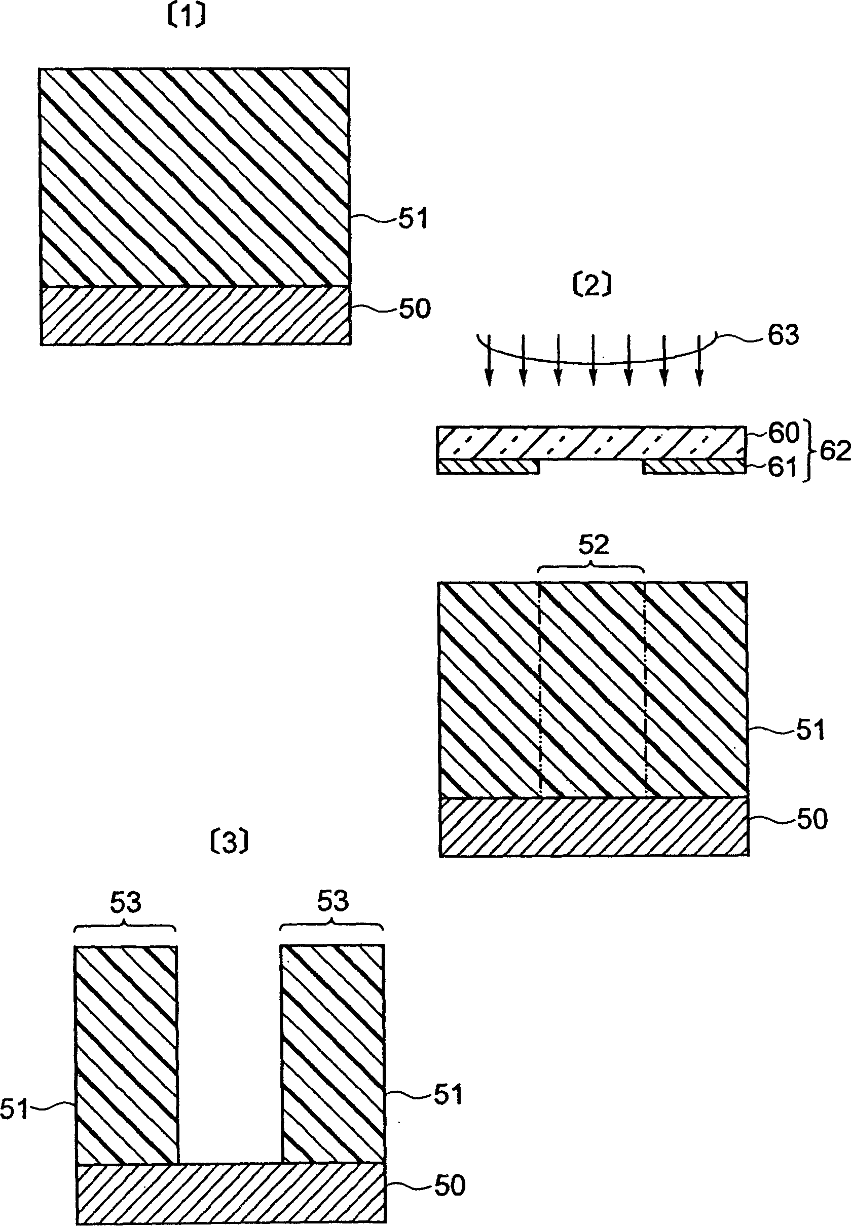
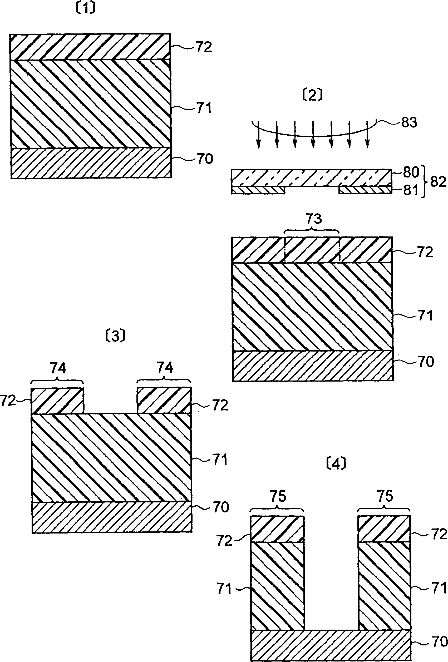
[0041] image 3 is a diagram for explaining the steps of an embodiment of the resist pattern forming method according to the present invention. Figure 4 so from Figure 4 [1] to Figure 4 Schematic sectional view of this embodiment in which steps are performed in the order of [3].

[0042] The following will refer to image 3 and Figure 4 [1] The outline of the embodiment is described.

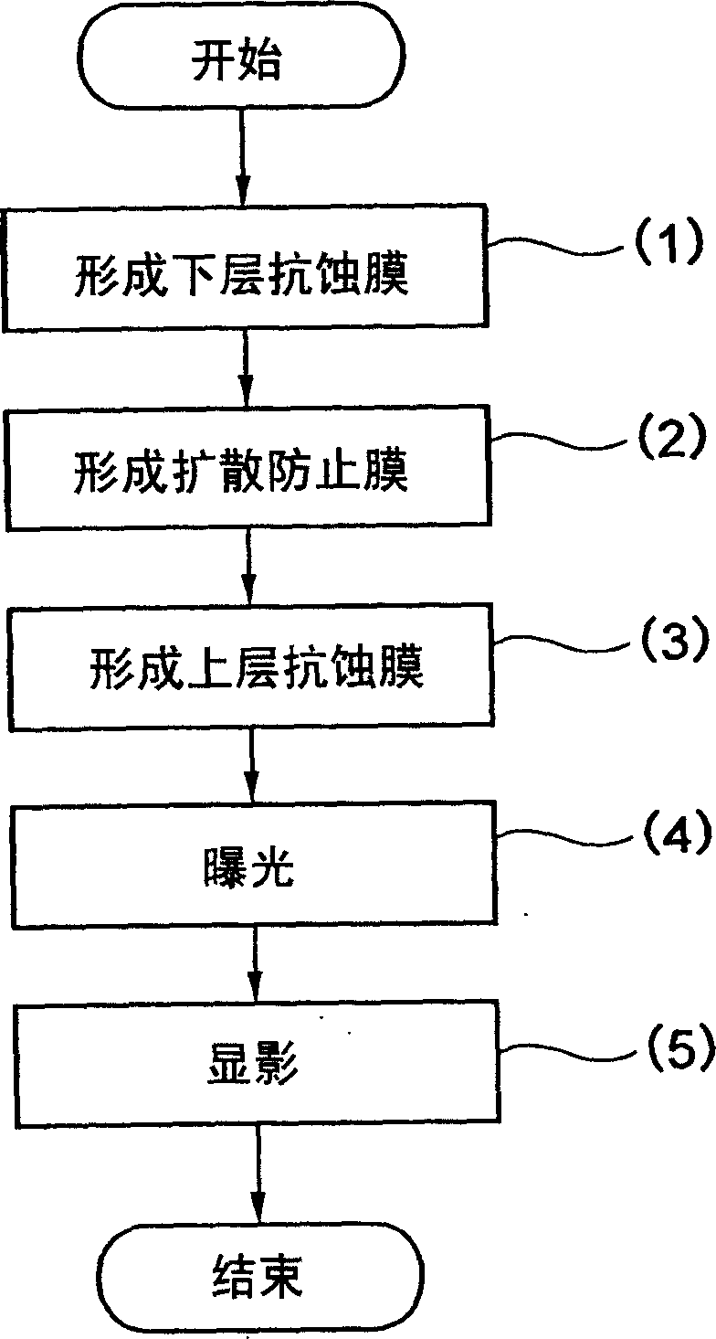
[0043] The resist pattern forming method according to this embodiment includes the steps of: forming an immediately lower resist film 11(1) on a substrate 10 to be etched; forming a diffusion preventing film 12(2) on the lower resist film 11; On the diffusion prevention film 12, form the upper layer resist film 13 (3); expose the lower layer resist film 11 and the upper layer resist film 13 simultaneously (4); and simultaneously expose the lower layer resist film 11 and the upper layer resist film 13 Develop (5).

[0044] Si, which is an etch resistance improving component for improvi...


PUM


Abstract

The invention discloses a method for forming a resist pattern using a double-layer resist process, which only needs a simple development step equivalent to that of a single-layer resist process. The method for forming a resist pattern includes the following steps: forming a lower resist film on a substrate; forming a diffusion prevention film on the lower resist film; forming an upper resist film on the diffusion prevention film; exposing the etching film and the upper resist film; and simultaneously developing the lower resist film and the upper resist film. Si, which is an etching resistance improving component, is contained only in the upper layer resist film and is not contained in the lower layer resist film. The diffusion prevention film prevents Si from diffusing from the upper layer resist film to the lower layer resist film and transmits light at the time of exposure, while having the property of being eliminated by a developer at the time of development.

Description

technical field [0001] The present invention relates to a resist pattern used for microprocessing in semiconductor manufacturing technology and the like, and more particularly to a method for forming a resist pattern. Background technique [0002] figure 1 is a schematic cross-sectional view describing the first conventional example of a resist pattern forming method, and steps from figure 1 [1] Proceed to figure 1 [3]. Description will be given below with reference to the accompanying drawings. [0003] The first traditional example is the single-layer resist process as the most common process. First, if figure 1 As shown in [1], sequential positive photoresists are coated on the substrate 50 having an oxide film to form a resist film having a film thickness of about 1 μm. Then, if figure 1 As shown in [2], a photomask 62 in which a light-shielding film 61 of a prescribed pattern is formed on a transparent substrate 60 is prepared. KrF laser light 63 is irradiated o...

Claims


Application Information

Patent Timeline
Patent Type & Authority Applications(China)
IPC IPC(8): G03F7/075G03F7/00G03F7/095G03F7/11G03F7/26H01L21/027
CPCG03F7/0757G03F7/095G03F7/11
Inventor 泷泽正晴
Owner ELPIDA MEMORY INC
Why Eureka
Try Eureka