Electronic circuit, system, nonvolatile memory and operating method thereof

A volatile memory and electronic circuit technology, applied in the field of semiconductor storage elements, can solve problems such as hindering process reduction in size and cost, low program efficiency, high operating voltage, etc., to achieve reduced programming and erase distribution, increased efficiency, The effect of accuracy optimization

Inactive Publication Date: 2005-08-17
MACRONIX INT CO LTD
View PDF0 Cites 5 Cited by
  • Summary
  • Abstract
  • Description
  • Claims
  • Application Information

AI Technical Summary

Problems solved by technology

[0004] Traditional programming uses superheated electron injection, which requires high operating voltages and consumes high energy
When the size of the non-volatile memory cell is reduced and the channel is relatively small, the high operating voltage leads to a punch-through effect, resulting in high leakage current and low program efficiency
Significant disadvantages in design and implementation of prior art two-bit memory cell non-volatile memory elements
In addition, prior art structures require a specially developed specification, hampering process efforts in size reduction and cost reduction

Method used


Image

  • Electronic circuit, system, nonvolatile memory and operating method thereof
  • Electronic circuit, system, nonvolatile memory and operating method thereof
  • Electronic circuit, system, nonvolatile memory and operating method thereof

Examples


Embodiment Construction
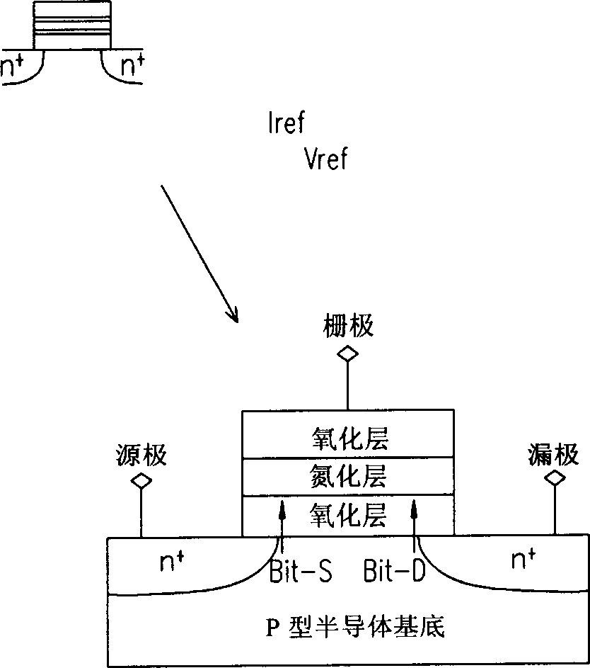
[0050] Table 1

[0051] exist figure 1 As in Table 1, when the first bit (bit D) is erased, electrons are injected into the gate of the non-volatile memory 10 programmed by hot hole injection nitride electron storage. Likewise, electrons are injected at the gate of the non-volatile memory when the second bit (bit S) is erased. And when the first bit (bit D) is programmed, holes are injected at the drain of the non-volatile memory, or electrons are reduced at the drain side. When programming the second bit (bit S), holes are injected at the source of the non-volatile memory, or electrons are dropped on the source side.

[0052] The trapping layer in at least one bit of the non-volatile memory is operable to retain electrons in an erased state, enabling the non-volatile memory to have a threshold voltage and a read current during a read operation. In addition, the comparator is used to receive the first input information generated by the read curren...


PUM


Abstract

One embodiment of the present-invention provides a system having a nonvolatile memory comprising a p type semiconductor substrate, an oxide layer over the p type semiconductor substrate, a nitride layer over the oxide layer, an additional oxide layer over the nitride layer, a gate over the additional oxide layer, two N+ junctions in the p type semiconductor layer, a source and drain respectively formed in the two N+ junctions, a first bit and a second bit in the nonvolatile memory, and accordingly at least two states of operation (i.e., erase and program) therefor. That is, one bit in the nonvolatile memory can either be in an erase state or program state. For erasing a bit, electrons are injected at the gate of the nonvolatile memory. For programming a bit, electric holes are injected or electrons are reduced for that bit. The present invention also provides a method for sensing and reading at least one bit in a nonvolatile memory comprising applying a bias voltage to the memory, detecting a threshold voltage or read current, comparing the threshold voltage with a reference voltage or comparing the read current with a reference current, and identifying the at least one bit as erased or programmed.

Description

technical field [0001] The present invention relates to a semiconductor storage device, and in particular to a non-volatile semiconductor storage unit, such as flash memory, and programming by hot hole injection Nitride electronstorage, PHINES) storage unit method. Background technique [0002] Memory elements for non-volatile data storage are currently widely used. Typical non-volatile semiconductor storage elements include read only memory (read only memory, ROM), programmable read only memory (programmable read only memory, PROM), erasable and programmable read only memory (erasable programmable read only memory, EPROM), electrically erasable programmable read-only memory (electrically erasable programmable readonly memory, EEPROM) and flash electrically erasable programmable read-only memory. [0003] Flash EEPROM is similar to EEPROM in that both can be programmed (that is, written) and can be electrically erased, but the addition can instantly erase all memory cells ...

Claims


Application Information

Patent Timeline
Patent Type & Authority Applications(China)
IPC IPC(8): G11C16/02G11C16/04G11C16/06H01L21/28H01L21/8247H01L27/115H01L29/788H01L29/792
CPCH01L29/7923H01L29/66833H01L21/28282H01L29/792G11C16/0475G11C16/10H01L29/40117
Inventor 叶致锴陈宏岳廖意瑛蔡文哲卢道政
Owner MACRONIX INT CO LTD
Why Eureka
Try Eureka