Eureka AIR delivers breakthrough ideas for toughest innovation challenges, trusted by R&D personnel around the world.

Ferromagnetic IV group based semiconductor, ferromagnetic III-V group based compound semiconductor, or ferromagnetic II-VI group based compound semiconductor, and method for adjusting their ferromagne

An adjustment method, semiconductor technology, applied to magnetic objects, magnetic materials, magnetic thin films, etc., can solve problems such as wavelength changes

Inactive Publication Date: 2005-08-24
JAPAN SCI & TECH CORP
View PDF1 Cites 3 Cited by
  • Summary
  • Abstract
  • Description
  • Claims
  • Application Information

AI Technical Summary

Problems solved by technology

So far, although the optical communication system that uses AlGaSb light-emitting components to cause light emission can be carried out, but at this time, wavelength changes caused by temperature changes will be generated, so Peltier components, etc. need to be used.

Method used


Image

  • Ferromagnetic IV group based semiconductor, ferromagnetic III-V group based compound semiconductor, or ferromagnetic II-VI group based compound semiconductor, and method for adjusting their ferromagne
  • Ferromagnetic IV group based semiconductor, ferromagnetic III-V group based compound semiconductor, or ferromagnetic II-VI group based compound semiconductor, and method for adjusting their ferromagne
  • Ferromagnetic IV group based semiconductor, ferromagnetic III-V group based compound semiconductor, or ferromagnetic II-VI group based compound semiconductor, and method for adjusting their ferromagne

Examples


Embodiment 1

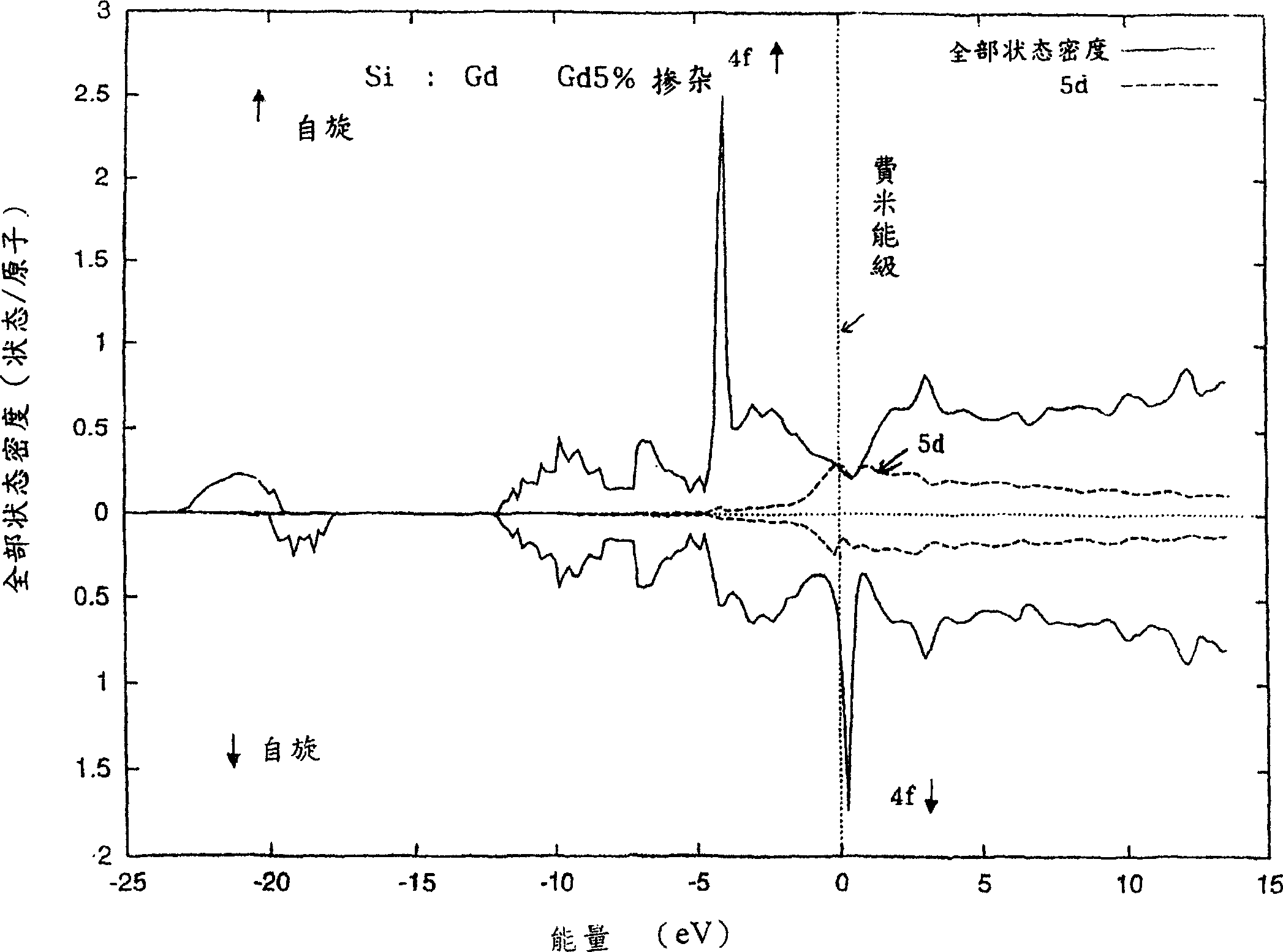
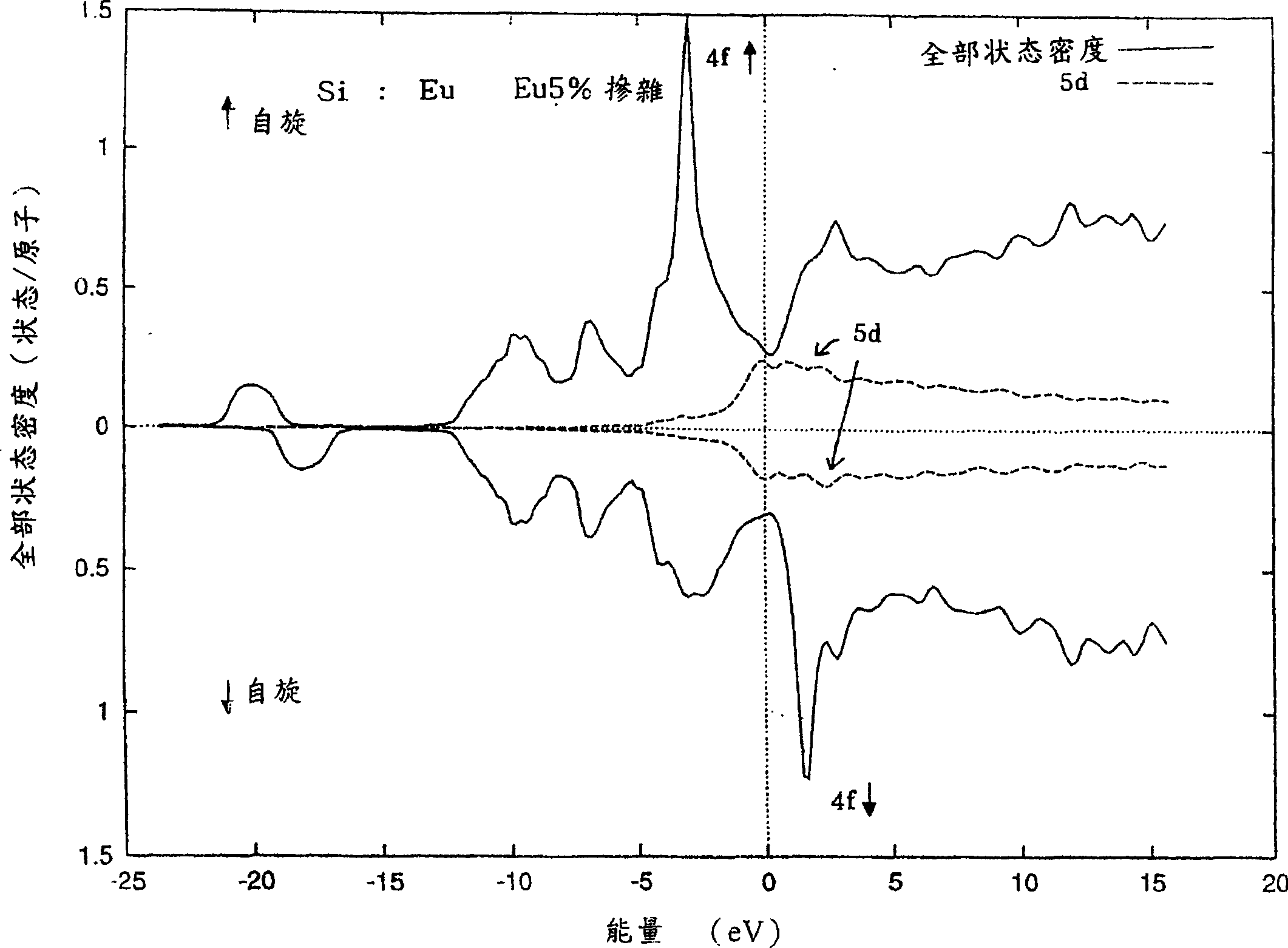
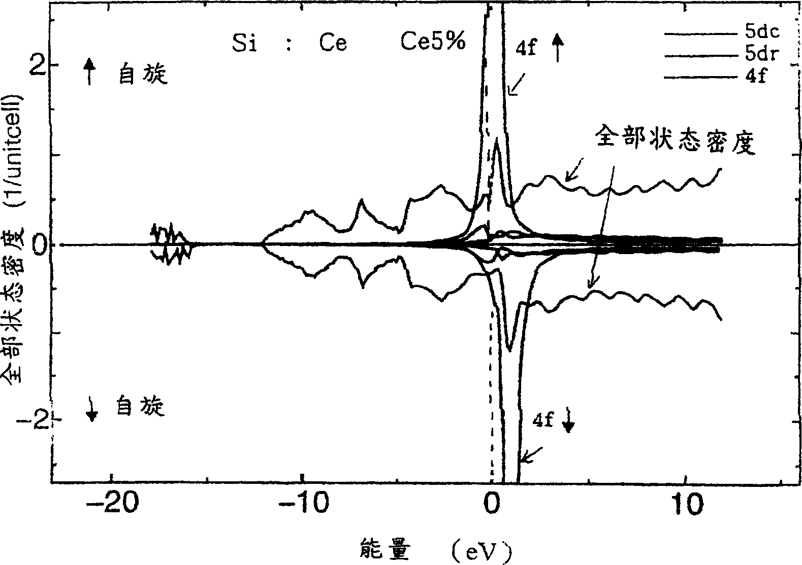
[0082] Fig. 9 shows the ferromagnetism transition temperature system when AlN is doped with 5 at% rare earth metals. It shows a higher ferromagnetic transition temperature of 300K or higher than room temperature. By selecting the type of rare earth metal, the ferromagnetic transition temperature can be adjusted, and a transparent ferromagnetic semiconductor that passes visible light can be obtained. Also, the ferromagnetic transition temperature (Tc) can be clearly known from experiments to be proportional to the path of the concentration (C) of the pre-mixed rare earth metal (Tc∞√C).

Embodiment 2

[0084] The ferromagnetic transition temperature when GaN has been doped with 5at% and 10at% rare earth metals is shown in Figure 10 . It shows a higher ferromagnetic transition temperature of 400K or higher than room temperature. By selecting the type of rare earth metal, the ferromagnetic transition temperature can be adjusted, and a transparent ferromagnetic semiconductor that passes visible light can be obtained.

Embodiment 3

[0086] The doping temperature of the donor oxygen and the ferromagnetic transition temperature when GaN has been doped with Gd 5at% are shown in Figure 11 . Although Gd-doped GaN alone does not exhibit ferromagnetism, it is evident that the ferromagnetic transition temperature can be adjusted by doping the donor oxygen to change the donor concentration.

[0087] effect

[0088]According to the present invention, only Ce, Pr, Nd, Pm, Sm, Eu, Gd, At least one metal selected from the group consisting of rare earth metal elements of Tb, Dy, Ho, Er, Tm, Yb and Lu, which has a higher ferromagnetism than room temperature due to the large magneto-optical effect available The ferromagnetic single crystal of the transition temperature, so the ferromagnetic semiconductor spintronic device material is used as the combination of ZnO or transparent conductive oxide (TCO) and optical fiber used as the n-type and p-type transparent electrodes that have been realized. Quantum computer or...


PUM


Abstract

Disclosed is a ferromagnetic group IV-based semiconductor or a ferromagnetic group III-V-based or group II-VI-based compound semiconductor, comprising a group IV-based semiconductor or a group III-V-based or group II-VI-based compound semiconductor, which contains at least one rare-earth metal element selected from the group consisting of Ce, Pr, Nd, Pm, Sm, Eu, Gd, Th, Dy, Ho, Er, Tm, Yb and Lu. The ferromagnetic characteristic of the ferromagnetic semiconductor is controlled by adjusting the concentration of the rare-earth metal element, combining two or more of the rare-earth metal elements or adding a p-type or n-type dopant.

Description

technical field [0001] The present invention relates to IV group semiconductors, III-V group compound semiconductors, or II-VI group compound semiconductors that can transmit from infrared light to ultraviolet rays, by making Ce, Pr, Nd, Pm, Sm, Ferromagnetic group IV system of single crystals that realize ferromagnetic properties by mixing crystals of at least one element selected from the group of rare earth metal elements such as Eu, Gd, Tb, Dy, Ho, Er, Tm, Yb, and Lu A semiconductor, a ferromagnetic III-V compound semiconductor, or a ferromagnetic II-VI compound semiconductor, and a method for adjusting the ferromagnetic properties of these semiconductors. Background technique [0002] If a single-crystal ferromagnetic thin film that transmits light and has ferromagnetic properties can be obtained, the optical isolator (isolator) required for a large amount of information transmission or high-density magnetic recording using light will become possible, and future Electr...

Claims


Application Information

Patent Timeline
IPC IPC(8): H01F1/40
CPCH01F1/40H01F1/405H01F1/0009H01F10/193H01F1/401H01F1/404H01F1/402G02F1/09C01F7/66
Inventor 吉田博荒木和也佐藤和则
Owner JAPAN SCI & TECH CORP
Why Eureka
Eureka Blog
Learn More