Epoxy resin composition for semiconductor encapsulation and semiconductor device using the same

A technology of epoxy resin and semiconductor, which is applied in the direction of semiconductor devices, semiconductor/solid-state device components, electric solid-state devices, etc., can solve separation problems, achieve the effects of preventing separation and cracking, high reliability, and good adhesion

Inactive Publication Date: 2005-10-05
NITTO DENKO CORP
View PDF2 Cites 3 Cited by
  • Summary
  • Abstract
  • Description
  • Claims
  • Application Information

AI Technical Summary

Problems solved by technology

Especially in the nickel-plated frame and heat sink, there is a problem that separation between the sealing resin part (cured resin) formed by the sealing material and the frame / heat sink occurs during package molding

Method used


Image

  • Epoxy resin composition for semiconductor encapsulation and semiconductor device using the same
  • Epoxy resin composition for semiconductor encapsulation and semiconductor device using the same
  • Epoxy resin composition for semiconductor encapsulation and semiconductor device using the same

Examples


Embodiment 1-13 and comparative example 1-5

[0111] The components shown in Tables 1 and 2 were mixed together in the proportions shown in the table. The mixture was heated (1 minute) at 80° C. using a mixing roll kneader, and thereby melt-kneaded. Subsequently, the melt was cooled, pulverized, and then tabletted. A target epoxy resin composition for semiconductor encapsulation was thus obtained.

[0112] Table 1

[0113] Example

[0114] Table 2

[0115] Example

[0116] Quartz powder in the whole

[0117] The adhesiveness and frame separation during molding of the epoxy resin compositions thus obtained in Examples and Comparative Examples were examined / evaluated. The results are shown in Tables 3 and 4.

[0118] adhesiveness

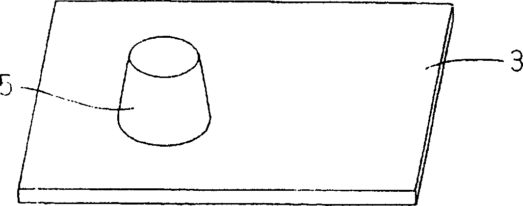
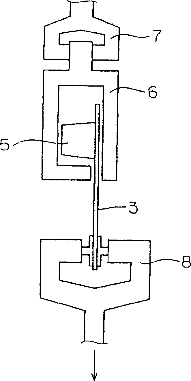
[0119] Each epoxy composition and metal frame plate was used to mold samples for adhesion testing by transfer molding (175°C x 2 minutes and 175°C x 5 hours for post-cure). Such as figure 1 As shown, this sample includes a metal frame plate 3 and a frustum...


PUM

PropertyMeasurementUnit
specific surface areaaaaaaaaaaa
softening pointaaaaaaaaaa

Abstract

An epoxy resin composition for semiconductor encapsulation which is for use in the resin encapsulation of semiconductor elements other than optical semiconductor elements including photoreceptors and light-emitting elements. This epoxy resin composition comprises the following ingredients (A) to (D) and has a content of ingredient (D) of 75-95% by weight based on the whole epoxy resin composition: (A) an epoxy resin, (B) a phenolic resin, (C) a specific release agent, and (D) an inorganic filler. The epoxy resin composition for semiconductor encapsulation which has improved adhesive force in application to metallic frame parts / heat radiation plates and can be inhibited from suffering separation from metallic frame parts / heat radiation plates during molding.

Description

technical field [0001] The present invention relates to an epoxy resin composition for semiconductor encapsulation which has improved adhesion when applied to a package frame and is capable of preventing separation between the encapsulation resin and the frame / radiation plate at the time of package molding . The present invention also relates to a semiconductor device using the composition. Background technique [0002] Semiconductor elements such as transistors, ICs, and LSIs are sealed in plastic packages and the like to prepare semiconductor devices that are protected from the surrounding environment and capable of controlling the semiconductor elements. Typical examples of this type of package include through-hole mount packages and surface mount packages. [0003] Recently, the processing speed and the degree of integration inside semiconductor devices such as LSI chips have become higher. In addition, there is a tendency to pursue higher packing density in order to ...

Claims


Application Information

Patent Timeline
Patent Type & Authority Applications(China)
IPC IPC(8): C08G59/62C08G59/68C08L63/02C08L83/04H01L23/00H01L23/29H01L23/495
CPCH01L23/293C08L63/00H01L2924/0002C08G59/686C08G59/621C08L83/04H01L23/49582Y10T428/31511Y10T428/31529C08L83/00H01L2924/00A23N15/00B26D3/26
Inventor 内田贵大清水雅人
Owner NITTO DENKO CORP
Why Eureka
Try Eureka