Capacitor coupled dynamic bias boosting circuit for a power amplifier

A technology for power amplifiers and amplifier circuits, which is applied in the direction of improving amplifiers to reduce temperature/power supply voltage changes, amplifiers, components of amplifiers, etc., and can solve problems such as high power consumption, no signal, no DC-coupled signal input, etc.

Inactive Publication Date: 2005-10-26
VLSI TECH LLC
View PDF2 Cites 4 Cited by
  • Summary
  • Abstract
  • Description
  • Claims
  • Application Information

AI Technical Summary

Problems solved by technology

This would inevitably lead to higher power dissipation at low power output levels in prior art circuits, thus resulting in an undesirable compromise in operating characteristics
[0005] The inventors have developed various techniques in the past including improved biasing circuits and bias boosting techniques, but these did not have the signal input to the amplifier circuit, or did not have a DC coupled signal input, which would have a negative impact on the biasing circuit and The operation of the coupled stage is unfavorable, making it design-limited

Method used


Image

  • Capacitor coupled dynamic bias boosting circuit for a power amplifier
  • Capacitor coupled dynamic bias boosting circuit for a power amplifier
  • Capacitor coupled dynamic bias boosting circuit for a power amplifier

Examples


Embodiment Construction

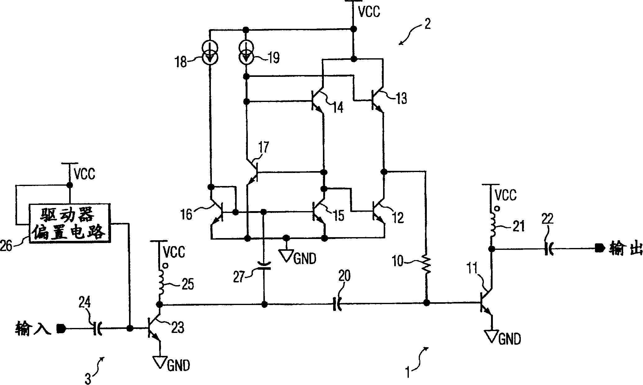
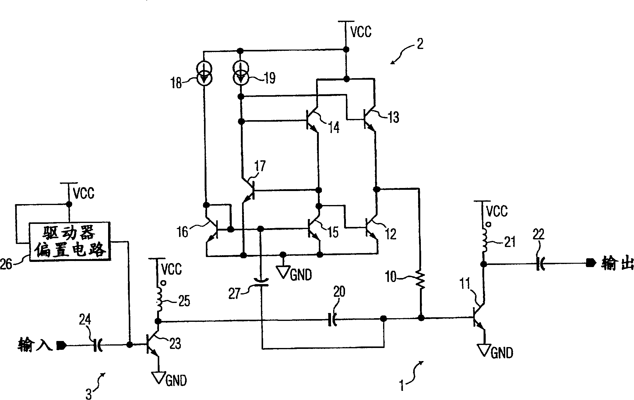
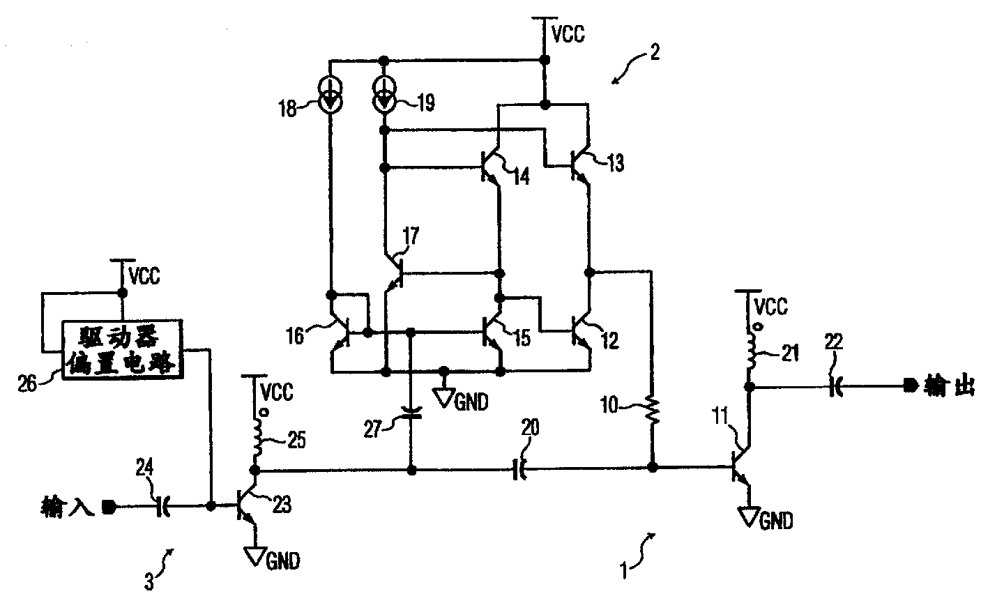
[0017] A brief schematic diagram of the high frequency amplifier circuit 1 according to the present invention is as figure 1 shown. The amplifier circuit includes an amplifier transistor 11 and a bias circuit 2 coupled to the base of the amplifier transistor 11 through a resistor 10 . The bias circuit 2 consists of coupling at V CC 6 bipolar transistors (12-17) and two current sources 18 and 19 between GND and GND will be further described below. An input coupling capacitor 20 is used to couple an input signal from the driver stage 3 of the amplifier to the base of the amplifier transistor 11 which is connected in a common emitter configuration and coupled through an inductor 21 at V CC and GND. The high frequency amplifier circuit 1 outputs from the collector of the transistor 11 through a capacitor 22 . The driver stage 3 includes a driver transistor 23 whose base input is coupled to a capacitor 24, a V CC connected, and connected to the output of capacitor 20. The dri...


PUM


Abstract

A power amplifier circuit includes an amplifying transistor and a dc bias circuit for biasing the amplifier transistor to obtain a conduction angle of at least about 180 DEG . The dc bias circuit includes a dynamic bias boosting circuit for increasing the dc bias current provided to the amplifying transistor by the dc bias current in direct proportion to an increase in the input signal provided to the power amplifier. An input to the dc bias circuit is coupled to a stage of the power amplifier circuit by a capacitor. The bias boosting circuit permits the power amplifier circuits to operate in Class B or Class AB with improved linearity, improved efficiency and reduced idle current.

Description

technical field [0001] The invention relates to the field of transistor amplifier circuits, in particular to a power amplifier with a bias boost circuit, which is used to enhance the linearity of the amplifier and reduce reactive current. Background technique [0002] This general-purpose type of amplifier is often used in high-frequency RF amplifiers, audio amplifiers, and other applications. In order to obtain a linear input-output relationship and high operating efficiency, the amplifier is typically operated at a conduction angle of approximately 180° (Class B) or slightly larger (Class AB) to avoid crossover distortion. [0003] Typically, such amplifiers require a DC bias circuit in order to establish the quiescent bias current in the amplifier circuit to ensure operation in class B or class AB mode. In the prior art, the bias is usually provided by a fixed current source, as described in US Pat. mode, as described in US Patent No. 5,548,248. [0004] However, in am...

Claims


Application Information

Patent Timeline
Patent Type & Authority Applications(China)
IPC IPC(8): H03F1/02H03F1/30
CPCH03F1/30H03F2200/18H03F1/0266H03F1/02
Inventor S·罗T·索拉蒂
Owner VLSI TECH LLC
Why Eureka
Try Eureka