

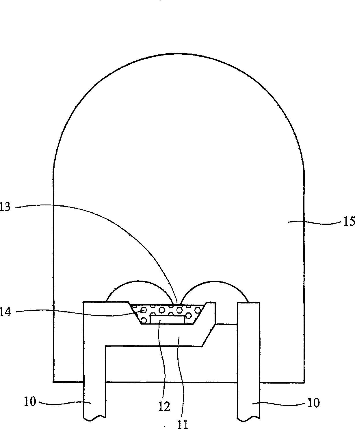
Light-emitting device and making method thereof, making system, packaging device and light emitting source, backlight module and display device
A technology for a light-emitting device and a manufacturing method, which is applied to the structure of a fluorescent layer and its production, and can solve the problems of uneven mixing of luminescent powder particles and adhesives, reduction of luminous efficiency and uniformity of luminous light, and easy rework. Ease of manufacture and cost reduction
- Summary
- Abstract
- Description
- Claims
- Application Information
AI Technical Summary
Problems solved by technology
Method used
Image

Examples
Embodiment 1
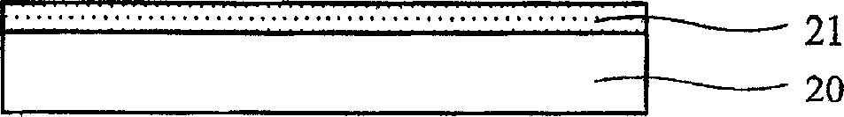
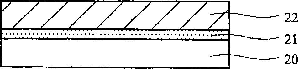
[0095] Firstly, the yttrium aluminum garnet (YAG for short) phosphor produced by Nichia Corporation and pure water are uniformly mixed with an ultrasonic oscillator to form a dispersion of yttrium aluminum garnet (YAG for short) phosphor ; Then put the produced gallium nitride (GaN) grains into this yttrium aluminum garnet (yttrium aluminum garnet, referred to as YAG) dispersion and let it stand for about 20 minutes, so that the yttrium aluminum garnet (yttrium aluminum garnet) in the dispersion The aluminum garnet (YAG for short) phosphor slowly deposits on the surface of the gallium nitride (GaN) grain, and at this time, the liquid level of the yttrium aluminum garnet (YAG for short) dispersion is higher than that of the gallium nitride (GaN) grain. grains, to form a uniform layer of yttrium aluminum garnet (yttrium aluminum garnet, referred to as YAG) phosphor particle distribution on the surface of gallium nitride (GaN) grains; then carry out the first drying step at a dryi...
Embodiment 2
[0097] Firstly, the yttrium aluminum garnet (YAG for short) phosphor produced by Nichia Corporation and alcohol are uniformly mixed with an ultrasonic oscillator to form a dispersion of the yttrium aluminum garnet (YAG for short) phosphor; Then put gallium nitride (GaN) crystal grains into the yttrium aluminum garnet (YAG for short) dispersion liquid and let it stand for about 20 minutes, so that the yttrium aluminum garnet (yttrium aluminum garnet, short for short) in the dispersion liquid YAG) phosphor is slowly deposited on the surface of the gallium nitride (GaN) grain, and at this time, the liquid level of the yttrium aluminum garnet (yttrium aluminum garnet, referred to as YAG) dispersion is higher than that of the gallium nitride (GaN) grain. A layer of uniform yttrium aluminum garnet (yttrium aluminum garnet, referred to as YAG) phosphor particle distribution is formed on the surface of gallium nitride (GaN) crystal grains; then the first drying step is carried out at a...
PUM
 Abstract
Description
Claims
Application Information