Operation scheme for spectrum shift in charge trapping non-volatile memory

A charge capture, operation and storage technology, applied in static memory, read-only memory, information storage, etc., can solve the problem of difficult storage of charge and achieve good durability and reliability

Active Publication Date: 2005-11-23
MACRONIX INT CO LTD
View PDF0 Cites 2 Cited by
  • Summary
  • Abstract
  • Description
  • Claims
  • Application Information

AI Technical Summary

Problems solved by technology

However, electrons with shallow energy levels have an important problem that the charge is difficult to preserve

Method used


Image

  • Operation scheme for spectrum shift in charge trapping non-volatile memory
  • Operation scheme for spectrum shift in charge trapping non-volatile memory
  • Operation scheme for spectrum shift in charge trapping non-volatile memory

Examples


Embodiment Construction

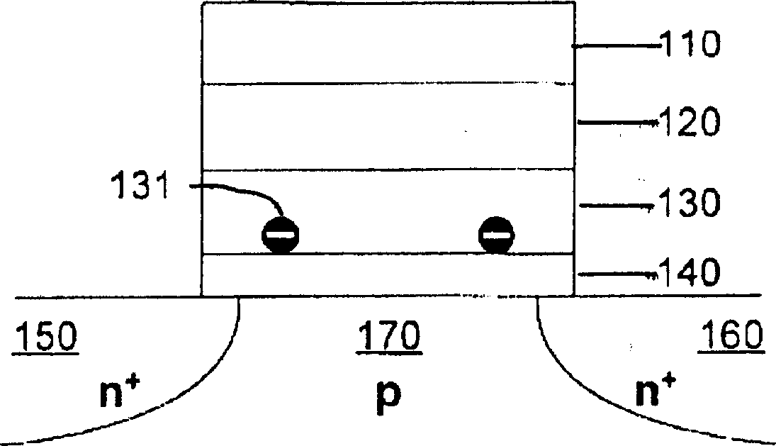
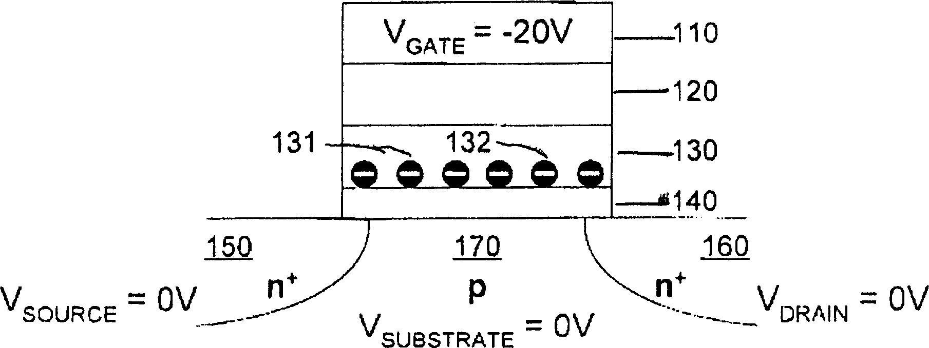
[0104] Please refer to FIG. 1A, which shows a schematic diagram of a charge trapping memory cell. The substrate in the figure includes n+ doped regions 150 and 160 , and a p-doped region 170 located between the n+ doped regions 150 and 160 . The memory cell further includes a bottom dielectric structure 140, a charge trapping structure 130, a top dielectric structure 120, and a gate 110, wherein the bottom dielectric structure 140 is located on the substrate , the charge trapping structure 130 is a bottom oxide layer (bottom oxide) located on the bottom dielectric structure 140, the top dielectric structure 120 is a top oxide layer (top oxide) located on the charge trapping structure 130, and the gate 110 is located on the top dielectric on the electrical structure 120 . The top dielectric layer is preferably a silicon dioxide (silicon dioxide) and silicon oxynitride (siliconoxynitride) with a thickness of about 5 to 10 nanometers, or other similar high dielectric constant ma...


PUM


Abstract

A method of operating a memory cell comprises applying a first procedure (typically erase) to establish a low threshold state including a first bias arrangement causing reduction in negative charge in the charge trapping structure, and a second bias arrangement tending to the induce balanced charge tunneling between the gate and the charge trapping structure and between the charge trapping structure in the channel. A second procedure (typically program) is used to establish a high threshold state in the memory cell, including a third bias arrangement that causes an increase in negative charge in the charge trapping structure.

Description

technical field [0001] The present invention relates to an electrically programmable and erasable nonvolatile memory, and more particularly to a charge trapping memory with a bias arrangement, in addition to boost and In addition to the operation of lowering the starting voltage, it can also be used to correct the charge in the memory. Background technique [0002] EEPROM technology is based on charge storage structures, such as EEPROM and flash memory, which are commonly used in various modern applications. Many memory cell structures are used in EEPROM and flash memory. Due to the simplicity and scalability of semiconductor manufacturing, interest in memory cell structures with charge-trapping dielectric layers has increased as the size of integrated circuits has shrunk. The memory cell structure with the charge trapping dielectric layer includes, for example, industrial names such as Nitride Read Only Memory (NROM), Silicon Oxide Nitride Oxide Silicon (SONOS) and PHINES...

Claims


Application Information

Patent Timeline
Patent Type & Authority Applications(China)
IPC IPC(8): H01L21/82H01L21/8246H01L21/8247
Inventor 吕函庭施彦豪谢光宇
Owner MACRONIX INT CO LTD
Why Eureka
Try Eureka