Test switching circuit for a high speed data interface

A high-speed data interface and switching circuit technology, applied in the direction of digital circuit testing, data exchange network, measuring electricity, etc., can solve the problems of increasing test costs, undetectable, programmable terminal resistance level errors, etc.

Inactive Publication Date: 2006-01-04
INFINEON TECH AG
View PDF0 Cites 12 Cited by
  • Summary
  • Abstract
  • Description
  • Claims
  • Application Information

AI Technical Summary

Problems solved by technology

The provision of an external loop has the following disadvantages: due to the insertion of multiple system tests, it increases the cost of testing; or the insertion of a single test loop causes the RF switch to be used, thus increasing the complexity of the load board.
[0015] like Figure 3 to Figure 5 The internal test circuit used to create an internal test loop in the prior art shown has several severe disadvantages
[0016] The first disadvantage is that if image 3 ,Figure 4, Figure 5 The arrangement shown makes it impossible to test either a final output stage, such as the differential amplifier stage D-AMP-C shown in Figure 4, and an input driver stage at the input, such as the Figure 5 The real function of the differential amplifier stage D-AMP-D shown in the figure
When a manufacturing error occurs in the differential amplifier stage D-AMP-C or in the differential ...

Method used


Image

  • Test switching circuit for a high speed data interface
  • Test switching circuit for a high speed data interface
  • Test switching circuit for a high speed data interface

Examples


Embodiment Construction

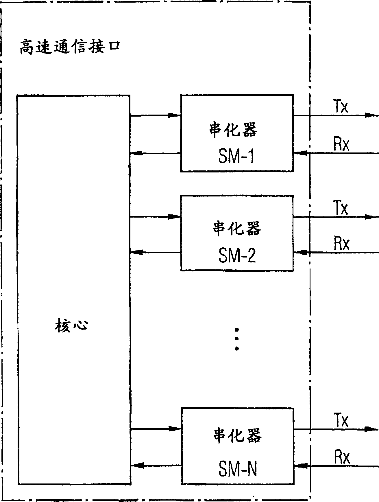
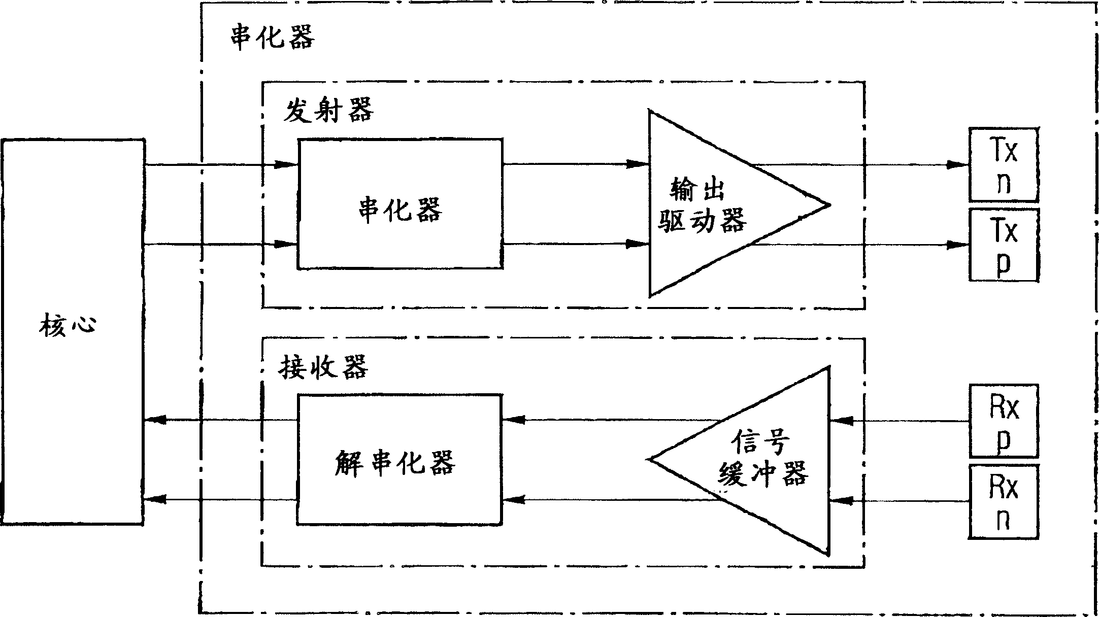
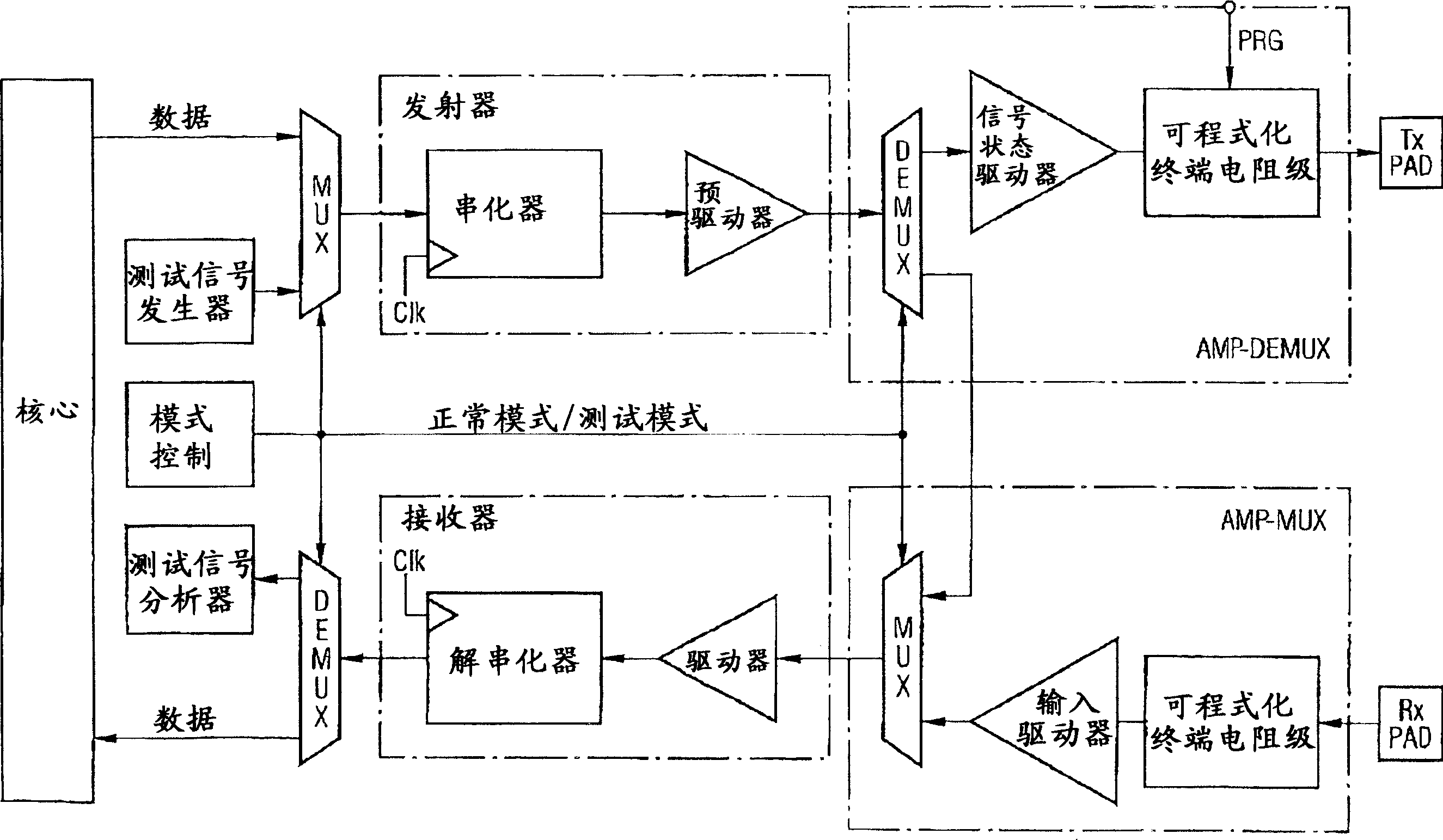
[0058] as Figure 6 Shown is a high-speed data interface 1 according to the present invention, which includes an internal data input 2 and an internal data output 3 to connect the high-speed data interface 1 to a data processing core 4 on an integrated circuit. The integrated circuit contains several high-speed data interfaces 1 . Each high-speed data interface has a transmit data output pin 4 and a receive data input pin 5 to connect the integrated circuit to an external circuit. A serial data stream is transmitted to the external circuit board through the output pin 4 , and a serial data receive stream is received through the receive data pin 5 . Such as Figure 6 In the preferred embodiment shown, the high-speed data interface includes a test signal generator 6 and a test signal analyzer 7 both of which can be controlled by a mode control unit 8 . In another alternative embodiment, the test signal generator 6, the test signal analyzer 7 and the mode control unit 8 are eq...


PUM


Abstract

Test switching circuit for a high speed data interface ( 1 ) of an integrated circuit comprising switching transistors (T 1 -T 6 ) which switch in a test mode a termination resistor output stage ( 15 ) of a data transmission signal path ( 17 ) to a termination resistor input stage ( 18 ) of a data reception signal path ( 25 ) to form an internal feedback test loop within said integrated circuit.

Description

technical field [0001] The present invention relates to a test switching circuit for a high speed data interface of an integrated circuit. Background technique [0002] High speed communication circuits transmitting data at rates in the 10Gbps range require closed feedback loops for testing purposes. figure 1 Represents a high-speed communication integrated circuit with a core for data processing and several high-speed interfaces. The high-speed data interface or serializer / deserializer (SERDES) module operates at a rate of up to 10Gbps. Each high-speed data interface (SERDES) is connected to a data transmission line (TX) and a data reception line (RX). The high-speed data interface transmits data via the data transmission line (TX) and receives data via the data reception line (RX). [0003] figure 2 Denotes a conventional high-speed data interface according to the prior art. The high-speed data interface includes a transmitter and a receiver. Such as figure 2 The ...

Claims


Application Information

Patent Timeline
IPC IPC(8): G01R31/28G01R31/317H03K17/687H04L12/26H04L25/12H04L29/10
CPCG01R31/31701G01R31/31716
Inventor J·阿尔古伊勒斯O·舒马彻尔
Owner INFINEON TECH AG
Why Eureka
Try Eureka