Semiconductor device and method for fabricating the same

A semiconductor and device technology, which is applied in the field of semiconductor devices and semiconductor device manufacturing, can solve the problems that it is difficult to reliably prevent the dielectric film from being damaged, and the dielectric film reduces the manufacturing output, so as to prevent the reduction of QSW, good electrical characteristics, and good The effect of coverage

Inactive Publication Date: 2006-01-04
FUJITSU SEMICON MEMORY SOLUTION LTD KANAGAWA
View PDF4 Cites 6 Cited by
  • Summary
  • Abstract
  • Description
  • Claims
  • Application Information

AI Technical Summary

Problems solved by technology

[0016] However, in simply producing an aluminum oxide film, it is difficult to reliably prevent the dielectric film from being damaged by hydrogen and water
Hydrogen and water damage to dielectric films reduces manufacturing yield

Method used


Image

  • Semiconductor device and method for fabricating the same
  • Semiconductor device and method for fabricating the same
  • Semiconductor device and method for fabricating the same

Examples


no. 1 example

[0067] The following will combine Figure 1 to Figure 22 The semiconductor device according to the first embodiment of the present invention and a method of manufacturing the semiconductor device are explained.

[0068] Semiconductor device

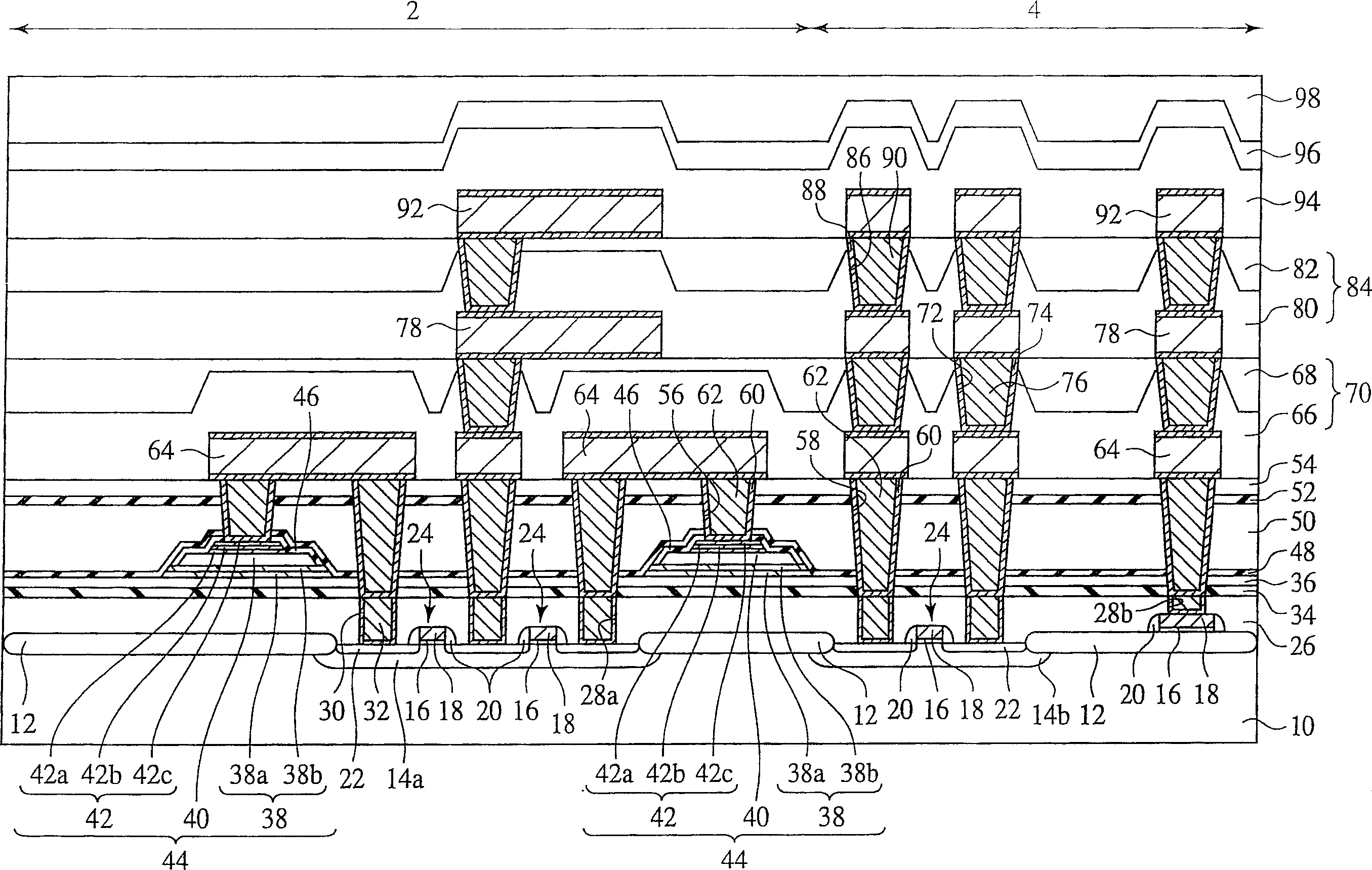
[0069] First, combine figure 1 To FIG. 4, the semiconductor device according to the present embodiment is explained. figure 1 It is a cross-sectional view of the semiconductor device according to this embodiment. in figure 1 In the figure, the memory cell area 2 is shown on the left side of the figure, and the peripheral circuit area 4 is shown on the right side of the figure.

[0070] Such as figure 1 As shown, a device isolation region 12 defining a device region is formed on a semiconductor substrate 10 such as silicon. Wells 14a and 14b are formed in the semiconductor substrate 10 in which the device isolation region 12 is formed.

[0071] A gate electrode (gate line) 18 is formed on the semiconductor substrate 10 on which the wells 1...

no. 2 example

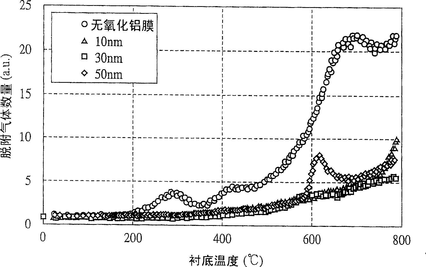
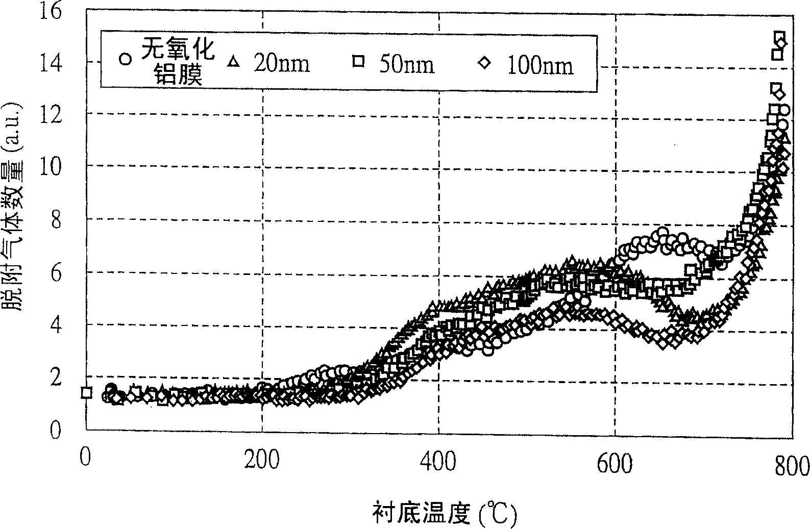
[0314] As described above, a flat barrier film (hydrogen diffusion preventing film) 52 for blocking the diffusion of hydrogen and water is formed on the capacitor, so that hydrogen and water can be surely prevented from reaching the capacitor 44.

[0315] However, when the barrier film 52 is simply formed, the exchange charge quantity Q of the capacitor 44 SW Usually reduced. The exchange charge quantity Q of the capacitor 44 SW This reduction is due to the large stress acting on the capacitor 44 when the ferroelectric film 40 forming the barrier film 52 and the barrier capacitor 44 is polarized.

[0316] The inventor of the present application conducted serious research and came up with a hydrogen / water diffusion preventing film with a function of blocking hydrogen and water diffusion and a stress relief layer for reducing the stress of the hydrogen / water diffusion preventing film to form a barrier film. The hydrogen / water diffusion preventing film for preventing the diffusion of...

no. 3 example

[0442] Next, a semiconductor device according to a third embodiment of the present invention and a method of manufacturing the semiconductor device will be explained with reference to FIGS. 35 to 37. FIG. 35 is a cross-sectional view of the semiconductor device according to the present embodiment. Figure 1 to Figure 34 The same components in the illustrated semiconductor devices and methods of manufacturing the semiconductor devices according to the first and second embodiments are represented by the same reference numerals, and the explanation of these reference numerals will not be repeated or simplified.

[0443]The main feature of the semiconductor device according to the present embodiment is that a plurality of hydrogen / water diffusion preventing films are stacked on each other with an intermediate layer formed therebetween, thereby forming a barrier film.

[0444] As shown in FIG. 35, a hydrogen / water diffusion preventing film 52 having a function of preventing the diffusio...


PUM


Abstract

The semiconductor device comprises a first insulation film 26 formed over a semiconductor substrate 10, first conductor plug 32 buried in a first contact hole 28 a formed down to a source / drain diffused layer 22, a capacitor 44 formed over the first insulation film 26, a first hydrogen diffusion preventing film 48 formed over the first insulation film 26, covering the capacitor 44, a second insulation film 50 formed over the first hydrogen diffusion preventing film and having the surface planarized, a second hydrogen diffusion preventing film 52 formed over the first hydrogen diffusion preventing film 26 and having the surface planarized, a second hydrogen diffusion preventing film 52 formed over the second insulation film 50, second conductor plug 62 buried in a second contact hole 56 formed down to the lower electrode 38 or the upper electrode 42 of the capacitor 44, a third conductor plug 62 buried in a third contact hole 58 formed down to the first conductor plug 32, and an interconnection 64 connected to the second conductor plug 62 or the third conductor plug 62.

Description

Technical field [0001] The present invention relates to a semiconductor device and a method of manufacturing a semiconductor device, and more particularly to a semiconductor device including a capacitor using a high dielectric constant substance or a ferroelectric substance as a dielectric film, and a method of manufacturing the semiconductor device. Background technique [0002] Recently, the use of a high dielectric constant substance or a ferroelectric substance as a dielectric film of a capacitor has attracted attention. [0003] However, when simply using high-permittivity materials and ferroelectric materials as the dielectric film of the capacitor, the oxygen in the dielectric film is often reduced by hydrogen in the subsequent steps after the dielectric film is formed, so the capacitor usually cannot have Good electrical properties. When the water contained in the interlayer insulating film or the like reaches the capacitor, the oxygen in the dielectric film is reduced by...

Claims


Application Information

Patent Timeline
Patent Type & Authority Applications(China)
IPC IPC(8): H01L27/105H01L21/8239
Inventor 永井孝一菊池秀明佐次田直也尾崎康孝
Owner FUJITSU SEMICON MEMORY SOLUTION LTD KANAGAWA
Why Eureka
Try Eureka