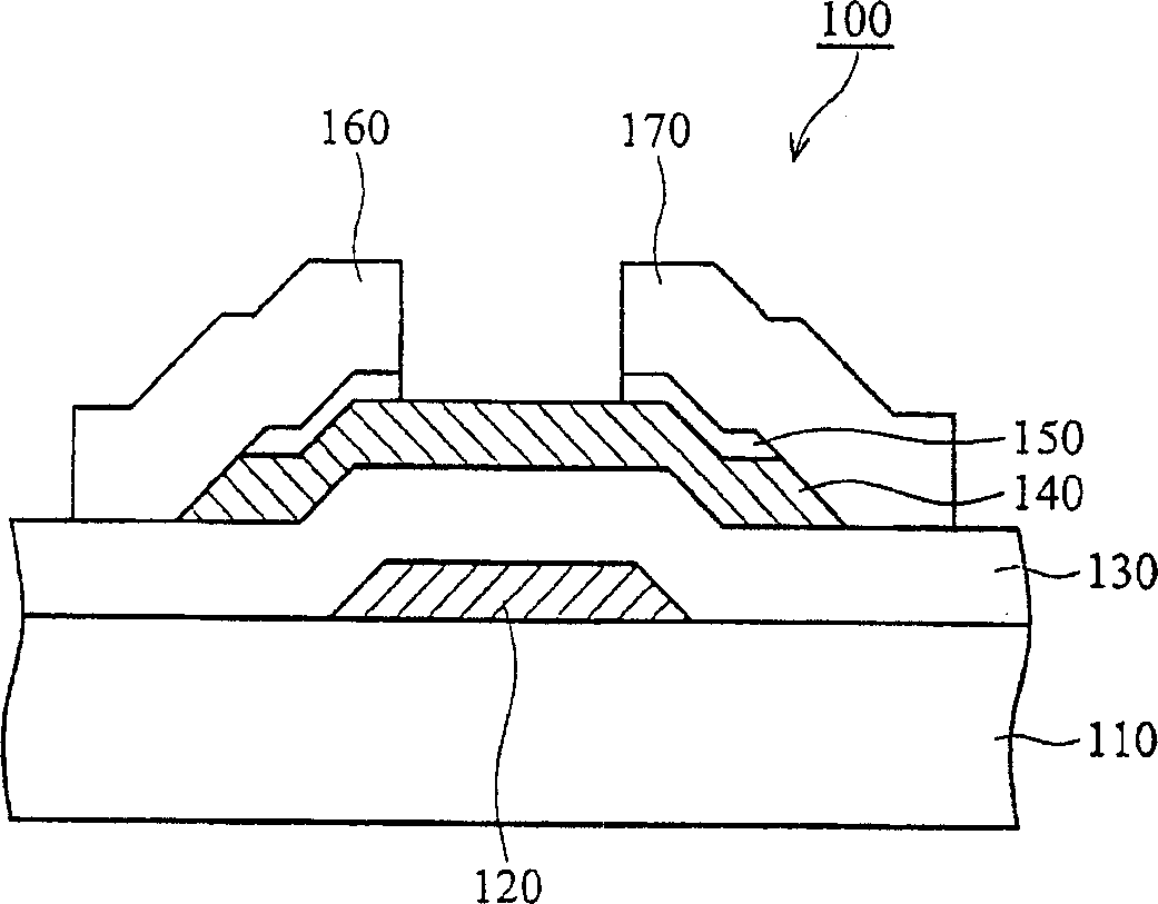
Switching element of pixel electrode, and manufacturing method
A technology of pixel electrode and switching element, which is applied to the switching element of pixel electrode and its manufacturing field, can solve the problems of rough surface of copper material, easy deformation of copper material, affecting the quality of elements, etc.
- Summary
- Abstract
- Description
- Claims
- Application Information
AI Technical Summary
Problems solved by technology
Method used
Image
Examples
no. 1 example
[0026] According to a preferred embodiment of the present invention, the method includes the following main steps.
[0027] Such as Figure 2A As shown, a material layer 215 is formed on the substrate 210 using a sputtering method. Wherein, the material layer 215 includes tantalum silicide, tantalum silicide nitride, titanium silicide, titanium silicide nitride, tungsten silicide, tungsten silicide nitride, and the thickness is approximately between 5 and 200 nanometers. The substrate 210 includes a glass substrate or a plastic substrate.
[0028] In other embodiments, the material layer 215 may be formed on the substrate 210 by using Atomic-Layer Deposition. Wherein, the material layer 215 includes tungsten carbide nitride, and the thickness is approximately between 5 and 200 nanometers. Next, a metal layer 217 is formed on the material layer 215 by chemical vapor deposition, electrochemical plating (ECP) or sputtering.
[0029] Such as Figure 2B As shown, a photolithog...
no. 2 example
[0034] According to a preferred embodiment of the present invention, the method includes the following main steps.
[0035] Such as Figure 3A As shown, a metal layer (not shown) is formed on a substrate 310 by chemical vapor deposition, electrochemical plating (ECP) or sputter deposition. Then, a photolithographic etching process is performed to form the gate 320 on the substrate 310 . The substrate 310 includes a glass substrate or a plastic substrate. The gate 320 includes copper, aluminum, silver, or alloys of the above metals, and has a thickness between about 100 and 500 nanometers.
[0036] Such as Figure 3B As shown, a diffusion barrier layer 325 is conformally formed on the gate 320 using sputtering. Wherein, the diffusion barrier layer 325 includes tantalum silicide, tantalum silicide nitride, titanium silicide, titanium silicide nitride, tungsten silicide, or tungsten silicide nitride, and the thickness is approximately between 5 and 200 nanometers.
[0037] I...
no. 3 example
[0042] According to a preferred embodiment of the present invention, the method includes the following main steps.
[0043] Such as Figure 4A As shown, a material layer 415 is formed on a substrate 410 using a sputtering method. Wherein, the material layer 415 includes tantalum silicide, tantalum silicide nitride, titanium silicide, titanium silicide nitride, tungsten silicide, or tungsten silicide nitride, and the thickness is approximately between 5 and 200 nanometers. The substrate 410 includes a glass substrate or a plastic substrate.
[0044] In other embodiments, the material layer 415 may be formed on the gate 420 by using Atomic-Layer Deposition. Wherein, the material layer 415 includes tungsten carbide nitride, and the thickness is approximately between 5 and 200 nanometers.
[0045] Next, a metal layer 417 is formed on the material layer 215 by chemical vapor deposition, electrochemical plating (ECP) or sputtering.
[0046] Such as Figure 4B As shown, a photol...
PUM
| Property | Measurement | Unit |
|---|---|---|
| Thickness | aaaaa | aaaaa |
| Thickness | aaaaa | aaaaa |
| Thickness | aaaaa | aaaaa |
Abstract
Description
Claims
Application Information


