Method for making organic thin film transistor and method for making liquid crystal display using same

A technology of organic thin films and transistors, applied in the field of manufacturing liquid crystal display devices

Active Publication Date: 2006-03-08
LG DISPLAY CO LTD
View PDF0 Cites 26 Cited by
  • Summary
  • Abstract
  • Description
  • Claims
  • Application Information

AI Technical Summary

Problems solved by technology

[0012] Therefore, the present invention aims to provide a method of manufacturing an organic thin film transistor and a method of manufacturing a liquid

Method used


Image

  • Method for making organic thin film transistor and method for making liquid crystal display using same
  • Method for making organic thin film transistor and method for making liquid crystal display using same
  • Method for making organic thin film transistor and method for making liquid crystal display using same

Examples


Embodiment Construction

[0029] Reference will now be made in detail to the preferred embodiments of the invention, examples of which are illustrated in the accompanying drawings.

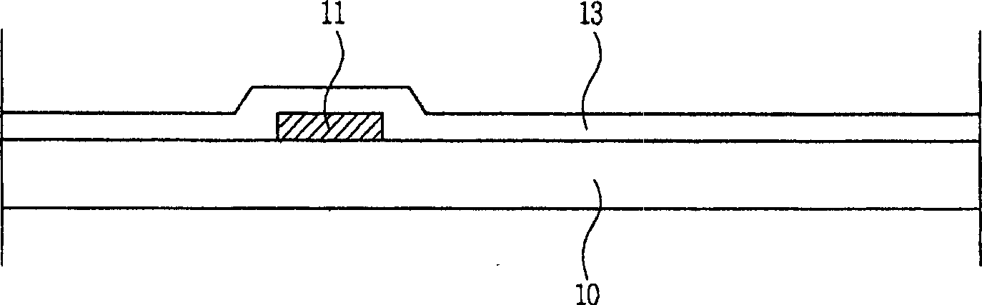
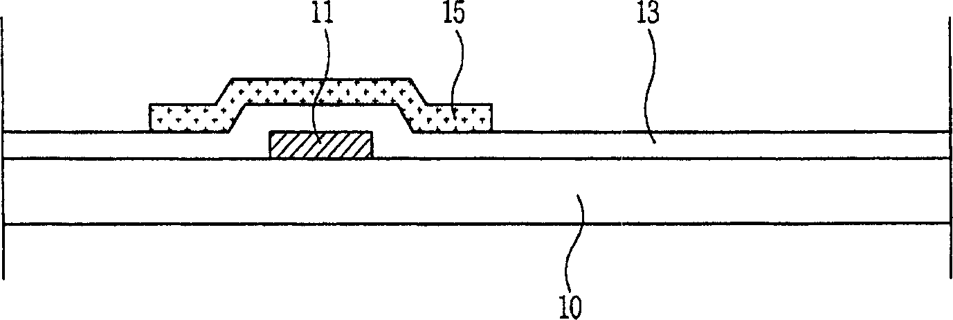
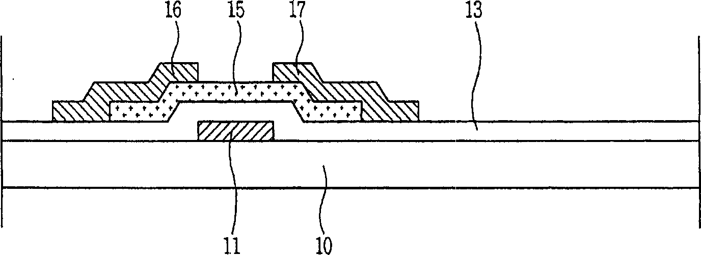
[0030] Figure 2A to Figure 2E is a cross-sectional view showing a method of manufacturing an OTFT according to an embodiment of the present invention, Figure 3A to Figure 3C is shown forming Figure 2B A cross-sectional view of the approach to the active layer of the OTFT shown in . Such as Figure 2A As shown, the method of manufacturing an OTFT includes preparing a first transparent substrate 110 . Specifically, a first conductive material is deposited and patterned to form the gate 111 .

[0031] The first conductive material may include one of copper (Cu), titanium (Ti), chromium (Cr), aluminum (Al), molybdenum (Mo), tantalum (Ta) and aluminum alloys, and may be formed by photolithography. The first conductive material is patterned. The photolithography process may include: a coating process of a photoresist fi...


PUM


Abstract

The invention provides a method for fabricating organic thin film transistor and a method for fabricating liquid crystal display device using the same. A method for fabricating an organic thin film transistor includes forming a gate electrode on a substrate, forming a gate insulating layer on the substrate including the gate electrode, forming an organic active pattern on the gate insulating layer using a rear exposing process, and forming source and drain electrodes on the organic active pattern.

Description

technical field [0001] The present invention relates to a method for manufacturing an organic thin film transistor, in particular to a method for manufacturing an organic thin film transistor using a rear exposing process (rear exposing process) to form an active layer and a method for manufacturing a liquid crystal display device using the method. Background technique [0002] With the development of polyacetylene (a conjugated organic polymer having semiconducting properties), organic semiconductors have been actively studied because of their ease of forming into a thin film type, and their superiority in flexibility, conductivity, and low production cost. Organic semiconductors can be used in electronic or optical devices. [0003] Among devices using semiconducting polymers, organic thin film transistors (OTFTs) using organic materials have been the focus of much ongoing research. Generally, an OTFT has a structure similar to that of a Si-TFT, however, in a semiconducto...

Claims


Application Information

Patent Timeline
IPC IPC(8): G02F1/136G02F1/133H01L29/786H01L21/027G03F7/20
CPCH01L29/66765G02F1/136227G02F1/1368H10K71/233H10K10/471H10K10/486H10K10/466
Inventor 徐铉植南大铉崔洛奉
Owner LG DISPLAY CO LTD
Why Eureka
Try Eureka