

Nano marking press
An embossing machine and nanotechnology, applied in printing machines, rotary printing machines, printing, etc., can solve the problems of no overlay alignment system, limited processing of single-layer nano-patterns, etc., and achieve automatic leveling and good flexibility Effect
- Summary
- Abstract
- Description
- Claims
- Application Information
AI Technical Summary
Problems solved by technology
Method used
Image

Examples
Embodiment Construction
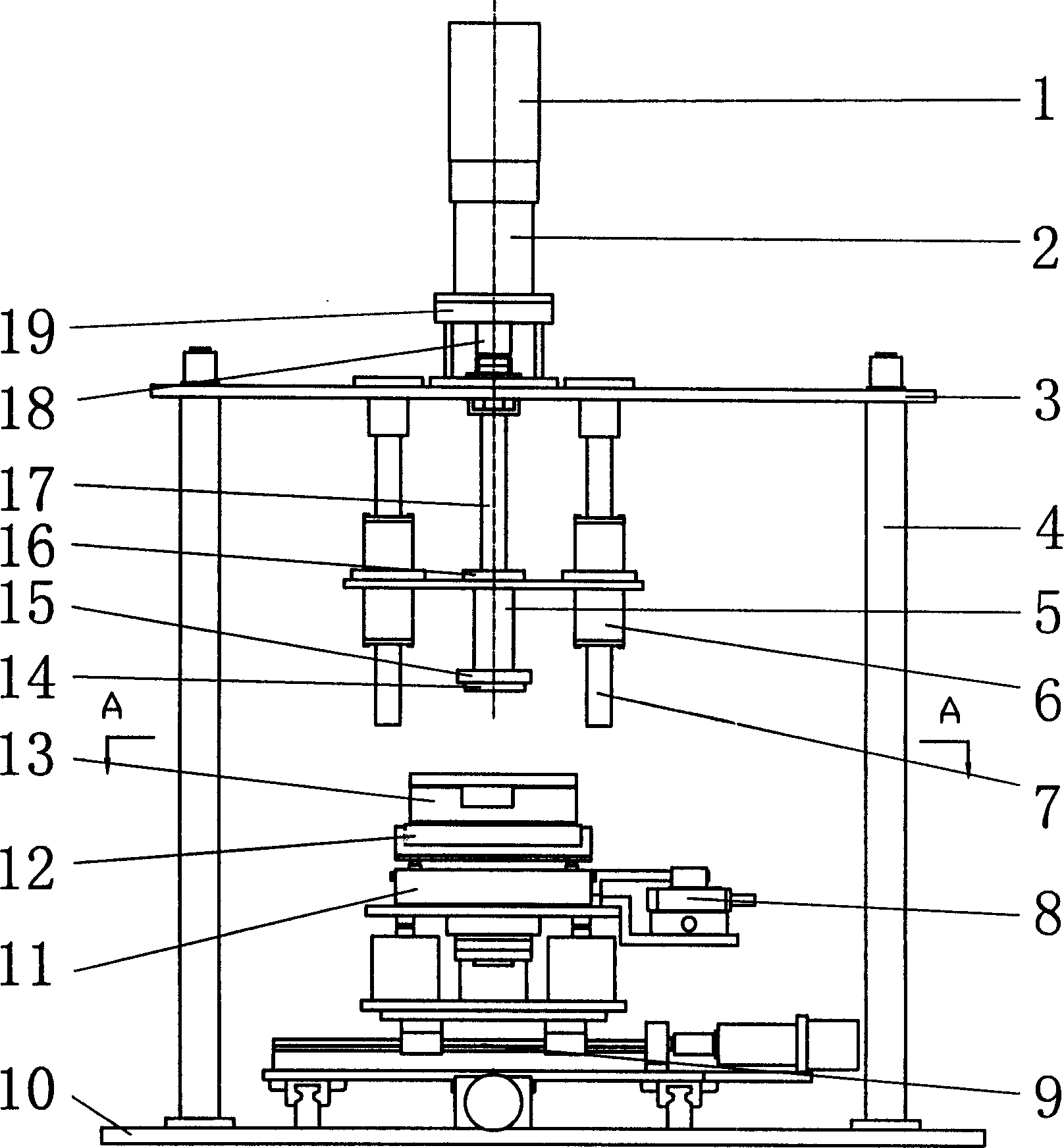
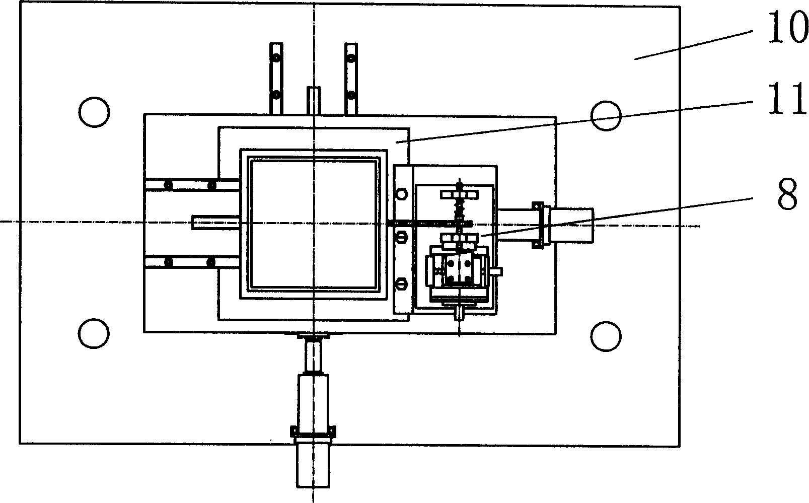
[0023] figure 1 , figure 2 Middle: 1-DC servo motor Z, 2-planetary gear reducer Z, 3-beam, 4-bracket, 5-fixed plate, 6-linear bearing, 7-guide rail Z, 8-rotary table, 9-X-Y thick Moving table, 10-base, 11-leveling device, 12-X-Y micro-moving table, 13-supporting plate, 14-template, 15-template clamping device, 16-transmission nut Z, 17-ball screw Z, 18-coupling Z, 19-support;
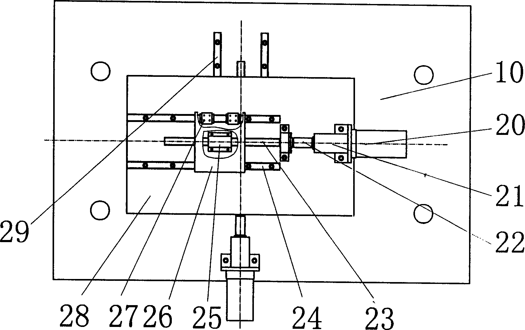
[0024] image 3 Middle: 20-stepper motor X, 21-planetary gear reducer X, 22-coupling X, 23-ball screw X, 24-linear guide X, 25-drive nut X, 26-plate X, 27- Slider X, 28-support plate, 29-Y direction coarse movement table;
[0025] Figure 4 Middle: 30-slider Y, 31-linear guide Y, 32-stepping motor Y, 33-planetary gear reducer Y, 34-coupling Y, 35-ball screw Y, 36-transmission nut Y, 37 - Tablet Y;
[0026] Figure 5 Middle: 38-cylindrical pin, 39-rotating rod, 40-first spring, 41-fixed plate, 42-a carriage, 43-pressure sensor, 44-base plate, 45-nut, 46-rotating shaft, 47-sleeve, 48-angular con...
PUM
 Abstract
Description
Claims
Application Information